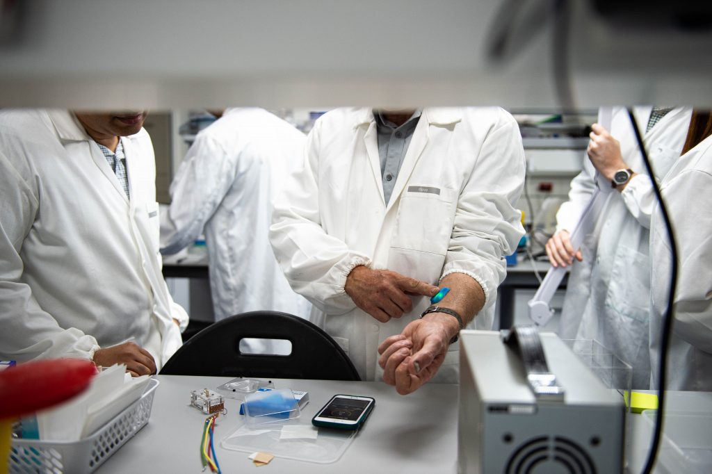
Accurate monitoring of a patient’s wellbeing relies on a network sensing and imaging equipment. Making these devices more accurate and easier to use increases the amount of information available to a patient, and makes the process far more comfortable.
Wearable sensors that sit on top of the skin are now commonplace, with researchers aiming to improving their accuracy and reducing their cost. Implantable devices are also widely used, transmitting or recording information directly from within the body.
Some groups are also looking at the “inbetween” class of devices – Microwearables that dip just below the skin’s surface to access more information than wearables, while not requiring a surgical procedures to be applied.
Novel polymer optical fibres are currently being investigated as blood pressure monitoring devices, they collect a variety of information, and they can be made to be biocompatible. MEMS or plasmonic devices, and a variety of other technologies can all be harnessed to produce sensors that are smaller, more accurate, and can serve multiple purposes. The result is a wave of micro and nanofabricated devices that can help the treatment of a patient.
(Image credit: Wearoptimo)

Photolithography is used to create a pattern on a substrate by shining light from a light source onto a photoresist that coats the surface of the substrate through a photomask and is followed by a development phase.
Depending on the complexity of a device’s design, various deposition, etching and lithography…
Reactive Ion Etching (RIE) is a method that combines both chemical and physical etching to allow isotropic and anisotropic material removal.
The etching process is carried out in a chemically reactive plasma containing positively and negatively charged ions generated from gases that are pumped into the reaction…
Plasma Enhanced Chemical Vapour Deposition (PECVD) uses a plasma to deposit a thin film of silicon dioxide or silicon nitrate onto a substrate. PECVD uses lower temperatures than the furnace systems to achieve an insulating layer on a variety of materials.
PECVD is used in optics, microelectronics, energy…
Electron-beam evaporation is a physical vapour deposition method for depositing thin films of metals, oxides and semiconductors in a high vacuum environment. Ultra high purity coating material is placed inside a vacuum chamber, typically as pellets in a crucible. Electron energy is used to heat these pellets,…
Annealing is a process that can reduce residual stress in a substrate that has accumulated during prior processes such as deposition.
The material is heated to high temperatures and allowed to cool at a controlled rate. This allows the material’s crystal structure to relax into a less intrinsically stressed state,…
Scanning Electron Microscopy (SEM) is the process whereby a tightly focused electron beam is scanned onto the surface to be imaged. As the primary electrons hit the atoms in the surface, a number of secondary electrons are emitted, and collected by the instrument’s detector, which assigns a level of grey…
Optical profilometry is a non-contact form of profilometry that can be used to characterise the surface steps and the roughness of a material.
Optical profilometry employs phase-shifting and/or vertical scanning interferometry to resolve the topology of complex 3D structures. The technique marries precision…
CNC milling is a conventional manufacturing technique that uses a computer to control a milling cutter.
It can be used to precisely machine geometries and features into a substrate, or to mill hot embossing stamps and jigs that may be used to fabricate microstructured features in devices.
The equipment typically…
Draw towers are used to create fibres, such as optical fibres, by heating and stretching a bulk material (or preform) to create long strands.
The design and composition of this preform results in different abilities of the fibres once drawn out, such as stronger fibres, more efficient data transmission, or a…
