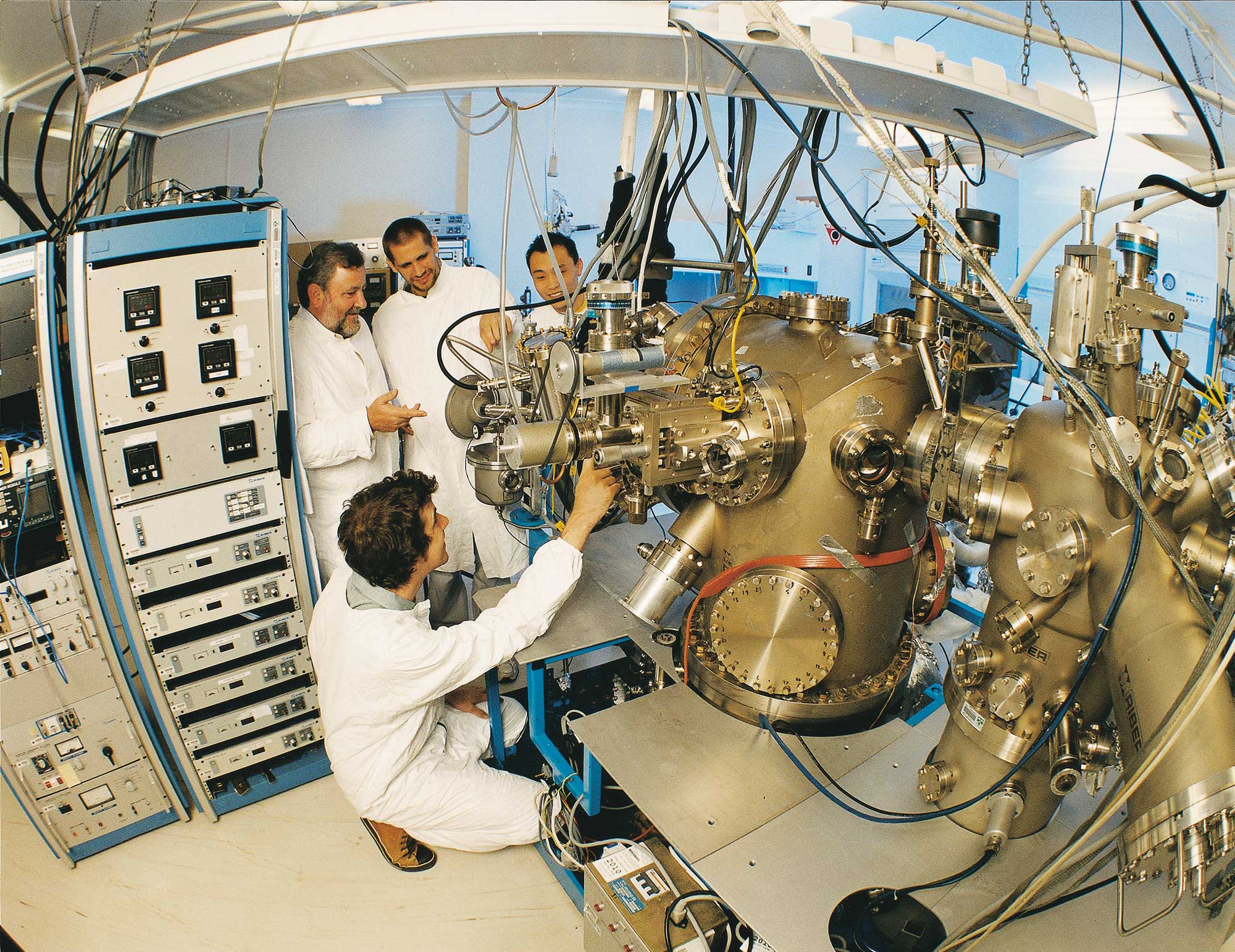
Nano Imprint Lithography
Nano Imprint Lithography
Nanoimprint lithography uses a transparent mould to deform a layer of photoresist into a desired topography. Light is then passed through the clear mould to cure the resist and make these deformations permanent. This technique relies on the accuracy of the mould but can be used to create many identical versions of the same structure.

List of available equipment
TOOL MAKE AND MODEL
KEY DIFFERENTIATOR
LOCATION
EVG 620
UV lithography and NIL exposure
ACT Node
Australian National University (ANU)
Description
Standard optical lithography and Nano-Imprint UV Lithography
Related Information
Process pieces up to 6 inch wafer with 1 micron resolution. Offers top-side alignment.
Tool Contact
horst.punzmann@anu.edu.au
EVG 620
Mask aligner and resist exposure system
QLD Node
University of Queensland
Description
Multilayer exposures of photoresists through a mask. Can resolve alignment marks down to 1µm and perform front and backside alignment on both 4 and 6 inch wafers.
Related Information
Any photoresist that can be exposed with 365 and 405nm.The system provides controlled pressure between the mask and the resist coated substrate. A shutter opens and closes providing a specific dose of UV to the exposed resist.
Tool Contact
anff@uq.edu.au
EVG 620
Mask aligner and resist exposure system with NIL capability
Melbourne Centre for Nanofabrication
VIC Node
Description
A high-resolution mask aligner with split-field microscopes that is capable of handling multiple wafer sizes with quick change-over time. Features back side alignment capability for mask aligning.
Related Information
Used for a variety of applications to transfer multiple layers of nanoscale patterns into photoresist films.Provides a minimum feature size of approximately 1 µm.
Tool Contact
mcn-enquiries@nanomelbourne.com
EVG 620…
Mask aligner and resist exposure system with NIL capability
SA Node
University of South Australia
Description
High resolution double side mask aligner with split-field microscopes which is capable of handling multiple wafer sizes with quick change-over time.Capable of processing ceramics, glasses, metals, polymers and semiconductors
Related Information
Used for a variety of applications to transfer multiple layers of nanoscale patterns into photoresist films.
Tool Contact
Simon.Doe@unisa.edu.au
TOOL MAKE AND MODEL
KEY DIFFERENTIATOR
LOCATION
EVG 620
UV lithography and NIL exposure
SA Node
University of South Australia
Description
Standard optical lithography and Nano-Imprint UV Lithography
Related Information
Process pieces up to 6 inch wafer with 1 micron resolution. Offers top-side alignment.
Tool Contact
horst.punzmann@anu.edu.au
TOOL MAKE AND MODEL
KEY DIFFERENTIATOR
LOCATION
EVG 620
Mask aligner and resist exposure system
SA Node
University of South Australia
Description
Multilayer exposures of photoresists through a mask. Can resolve alignment marks down to 1µm and perform front and backside alignment on both 4 and 6 inch wafers.
Related Information
Any photoresist that can be exposed with 365 and 405nm.The system provides controlled pressure between the mask and the resist coated substrate. A shutter opens and closes providing a specific dose of UV to the exposed resist.
Tool Contact
anff@uq.edu.au
TOOL MAKE AND MODEL
KEY DIFFERENTIATOR
LOCATION
EVG 620
Mask aligner and resist exposure system with NIL capability
SA Node
University of South Australia
Description
A high-resolution mask aligner with split-field microscopes that is capable of handling multiple wafer sizes with quick change-over time. Features back side alignment capability for mask aligning.
Related Information
Used for a variety of applications to transfer multiple layers of nanoscale patterns into photoresist films.Provides a minimum feature size of approximately 1 µm.
Tool Contact
mcn-enquiries@nanomelbourne.com
TOOL MAKE AND MODEL
KEY DIFFERENTIATOR
LOCATION
EVG 620…
Mask aligner and resist exposure system with NIL capability
SA Node
University of South Australia
Description
High resolution double side mask aligner with split-field microscopes which is capable of handling multiple wafer sizes with quick change-over time.Capable of processing ceramics, glasses, metals, polymers and semiconductors
Related Information
Used for a variety of applications to transfer multiple layers of nanoscale patterns into photoresist films.
Tool Contact
Simon.Doe@unisa.edu.au
