
Spin coating and wafer development
Spin coating and wafer development
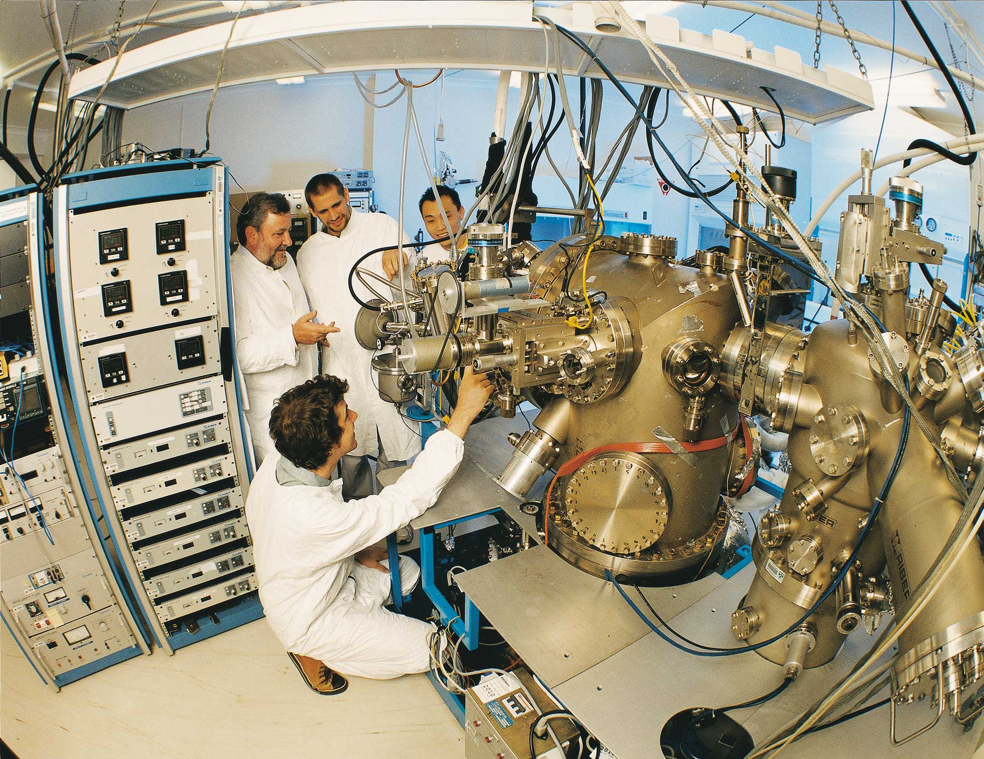
Spin coaters are capable of applying uniform thickness polymer films, such as a resist to substrates. Resist is essential for many types of lithography, such as UV lithography. Resists are termed either positive or negative — this denotes whether, when cured, chemical bonds are made or broken, and therefore whether the sections of resist that remain are either the true pattern, or it’s inverse. This selection must be considering etching or deposition stages that may follow as it will help to make.
List of available equipment
TOOL MAKE AND MODEL
KEY DIFFERENTIATOR
LOCATION
EVG 101 Spin/Spray resist coater
Spin and spray coating
SA Node
University of South Australia
Description
This is a spin and spray coater, which is used in micro- and nanofabrication processes to apply thin uniform films of photoresist, polymeric coatings or other materials onto a substrate using spin or spray coating technique.
Related Information
Capable of applying uniform thickness polymer films, such as a resist to substrates a “Gyrset” to help achieve uniformity, especially on square and rectangular substrates and to minimise edge bead build up.
Tool Contact
Simon.Doe@unisa.edu.au
EVG 105 Bake Module
Photolithography thermal curing
University of Western Australia
WA Node
Description
Softbake, post-exposure bake and hardbake processes. Programmable proximity pins provide the best available control of resist hardening processes and temperature profiles
Related Information
Process up to 300 mm wafer sizes or up to four 100 mm wafers at the same time
Tool Contact
anff-wa@uwa.edu.au
Laurell WS-400A
Spin coater for ink coatings
Materials Node
University of Newcastle
Description
Used to produce thin films on small substrates. The sample is placed onto a vacuum chuck and rotated at thousands of revolutions per minute whilst ink is deposited onto the surface. The majority of the ink is removed due to the rotation but what's left is an extremely thin, uniform film.
Related Information
Typical sample sizes are 1-2 cm2. Speeds from 200 to 8000 rpm are possible.
Tool Contact
anff@newcastle.edu.au
PicoTRACK PCT-150RRE
Automated spin-coating and wafer developing system
Melbourne Centre for Nanofabrication
VIC Node
Description
A fully automated system for wafer processing which includes spin coating, HMDS application, baking, and development.The system is well suited to batch scale production, providing high process performance and consistency in coating and development.
Related Information
Substrate size - 4 and 6 inch wafers. Batch process size - up to 25 wafers at a time. Resist system used - AZ 1512 and AZ 4562 photoresists to coat wafers and AZ 400K for development.
Tool Contact
mcn-enquiries@nanomelbourne.com
PM-Plast Delta 15
Mask Cleaning tool
NSW Node
University of Sydney
Description
Automated single wafer cleaning tool
Related Information
Primarily dedicated to mask cleaning
Tool Contact
rpf.queries@sydney.edu.au
Rite Track SVG 88
Spin coater and developer
NSW Node
University of Sydney
Description
A fully automated system for spin coating, HMDS application, baking, and development. The system is well suited to batch scale production, providing high process performance and consistency in coating and development.
Related Information
The system can process 4 and 6 inch wafers, and is capable of running 25 wafers at a time. Auto dispense of resist (standard SPR660). MF26 developer.
Tool Contact
rpf.queries@sydney.edu.au
SSE OPTIcoat ST22
Resist developer
Griffith University
QLD Node
Description
Uses a vacuum chuck to spin the wafer whilst a specific amount of photoresist is deposited on the surface of the substrate. Spin speeds and volumes are variable to allow for different thickness and uniformity requirements.
Related Information
An essential part of photolithography.
Tool Contact
glenn.walker@griffith.edu.au
Suss Delta 80 Spin Coater
Spin coater
SA Node
University of South Australia
Description
This is a spin coater, which is used in micro- and nanofabrication processes to apply thin uniform films of photoresist, polymeric coatings or other materials onto a substrate using spin coating technique.
Related Information
Capable of applying uniform thickness polymer films, such as a resist to substrates a “Gyrset” to help achieve uniformity, especially on square and rectangular substrates and to minimise edge bead build up.
Tool Contact
Simon.Doe@unisa.edu.au
Suss Delta RC80+ Spin Coater
Spin coater
Melbourne Centre for Nanofabrication
VIC Node
Description
Spin coater set up to process 4-inch wafers and also features a hot plate.
Related Information
high uniformity spin coater.
Tool Contact
mcn-enquiries@nanomelbourne.com
TOOL MAKE AND MODEL
KEY DIFFERENTIATOR
LOCATION
EVG 101 Spin/Spray resist coater
Spin and spray coating
Melbourne Centre for Nanofabrication
VIC Node
Description
This is a spin and spray coater, which is used in micro- and nanofabrication processes to apply thin uniform films of photoresist, polymeric coatings or other materials onto a substrate using spin or spray coating technique.
Related Information
Capable of applying uniform thickness polymer films, such as a resist to substrates a “Gyrset” to help achieve uniformity, especially on square and rectangular substrates and to minimise edge bead build up.
Tool Contact
Simon.Doe@unisa.edu.au
TOOL MAKE AND MODEL
KEY DIFFERENTIATOR
LOCATION
EVG 105 Bake Module
Photolithography thermal curing
Melbourne Centre for Nanofabrication
VIC Node
Description
Softbake, post-exposure bake and hardbake processes. Programmable proximity pins provide the best available control of resist hardening processes and temperature profiles
Related Information
Process up to 300 mm wafer sizes or up to four 100 mm wafers at the same time
Tool Contact
anff-wa@uwa.edu.au
TOOL MAKE AND MODEL
KEY DIFFERENTIATOR
LOCATION
Laurell WS-400A
Spin coater for ink coatings
Melbourne Centre for Nanofabrication
VIC Node
Description
Used to produce thin films on small substrates. The sample is placed onto a vacuum chuck and rotated at thousands of revolutions per minute whilst ink is deposited onto the surface. The majority of the ink is removed due to the rotation but what's left is an extremely thin, uniform film.
Related Information
Typical sample sizes are 1-2 cm2. Speeds from 200 to 8000 rpm are possible.
Tool Contact
anff@newcastle.edu.au
TOOL MAKE AND MODEL
KEY DIFFERENTIATOR
LOCATION
PicoTRACK PCT-150RRE
Automated spin-coating and wafer developing system
Melbourne Centre for Nanofabrication
VIC Node
Description
A fully automated system for wafer processing which includes spin coating, HMDS application, baking, and development.The system is well suited to batch scale production, providing high process performance and consistency in coating and development.
Related Information
Substrate size - 4 and 6 inch wafers. Batch process size - up to 25 wafers at a time. Resist system used - AZ 1512 and AZ 4562 photoresists to coat wafers and AZ 400K for development.
Tool Contact
mcn-enquiries@nanomelbourne.com
TOOL MAKE AND MODEL
KEY DIFFERENTIATOR
LOCATION
PM-Plast Delta 15
Mask Cleaning tool
Melbourne Centre for Nanofabrication
VIC Node
Description
Automated single wafer cleaning tool
Related Information
Primarily dedicated to mask cleaning
Tool Contact
rpf.queries@sydney.edu.au
TOOL MAKE AND MODEL
KEY DIFFERENTIATOR
LOCATION
Rite Track SVG 88
Spin coater and developer
Melbourne Centre for Nanofabrication
VIC Node
Description
A fully automated system for spin coating, HMDS application, baking, and development. The system is well suited to batch scale production, providing high process performance and consistency in coating and development.
Related Information
The system can process 4 and 6 inch wafers, and is capable of running 25 wafers at a time. Auto dispense of resist (standard SPR660). MF26 developer.
Tool Contact
rpf.queries@sydney.edu.au
TOOL MAKE AND MODEL
KEY DIFFERENTIATOR
LOCATION
SSE OPTIcoat ST22
Resist developer
Melbourne Centre for Nanofabrication
VIC Node
Description
Uses a vacuum chuck to spin the wafer whilst a specific amount of photoresist is deposited on the surface of the substrate. Spin speeds and volumes are variable to allow for different thickness and uniformity requirements.
Related Information
An essential part of photolithography.
Tool Contact
glenn.walker@griffith.edu.au
TOOL MAKE AND MODEL
KEY DIFFERENTIATOR
LOCATION
Suss Delta 80 Spin Coater
Spin coater
Melbourne Centre for Nanofabrication
VIC Node
Description
This is a spin coater, which is used in micro- and nanofabrication processes to apply thin uniform films of photoresist, polymeric coatings or other materials onto a substrate using spin coating technique.
Related Information
Capable of applying uniform thickness polymer films, such as a resist to substrates a “Gyrset” to help achieve uniformity, especially on square and rectangular substrates and to minimise edge bead build up.
Tool Contact
Simon.Doe@unisa.edu.au
TOOL MAKE AND MODEL
KEY DIFFERENTIATOR
LOCATION
Suss Delta RC80+ Spin Coater
Spin coater
Melbourne Centre for Nanofabrication
VIC Node
Description
Spin coater set up to process 4-inch wafers and also features a hot plate.
Related Information
high uniformity spin coater.
Tool Contact
mcn-enquiries@nanomelbourne.com