ANFF Western Australia
Home > Locations
Overview

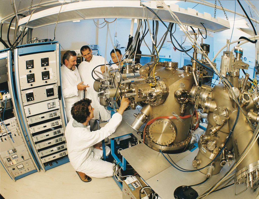
ANFF WA provides a wealth of knowledge in advanced microelectronic, optoelectronic, and photonic materials, devices and systems. The node runs a complete, vertically integrated facility, from materials growth, through device design, fabrication and testing, to packaging and subsystem assembly.

The WA node is based at the University of Western Australia, Crawley. It incorporates the Microelectronics Research Group (MRG) in the School of Electrical, Electronic & Computer Engineering, led by Prof Lorenzo Faraone. The MRG provides a wealth of knowledge on advanced microelectronic, optoelectronic, and photonic materials, devices and systems.

Node Competencies

Specialist fields: Semiconductor optoelectronics; II-VI semiconductor growth; Micro- and nano- electro-mechanical-systems (MEMS and NEMS); Advanced sensors.

Flagship Facilities and capabilities: Molecular beam epitaxy, Nanoindentation, DLTS, MEMS characterisation facilities.

Contact

Node Director: Prof Lorenzo Faraone
Email: Lorenzo.faraone@uwa.edu.au
Phone: +61 8 6488 3104

Facility Manager: Prof Mariusz Martyniuk
Email: mariusz.martyniuk@uwa.edu.au
Phone: +61 8 6488 1905

Location
University of Western Australia
Address

School of Electrical, Electronic & Computer Engineering,
Room 4.17, M018, The University of Western Australia
35 Stirling Highway, Crawley WA 6009

Equipment
Deposition
Custom Dual Chamber Thermal Evaporator
Custom dual chamber system for multi-material thermal evaporation
University of Western Australia WA Node
Technique
Thermal evaporation
Description
Custom made dual chamber thermal evaporator for deposition of metal and non-metal materials with high deposition rate and high purity.
Related Information
Materials: Cr, Au, Al, Ag, MgF₂, Ge, and certain other materials upon request.
Tool Contact
anff-wa@uwa.edu.au
Custom Indium Thermal Evaporator
Custom system for Indium (In) thermal evaporation
University of Western Australia WA Node
Technique
Thermal evaporation
Description
Thermal evaporator designed for Indium deposition (In dedicated)
Related Information
Exclusively for Indium deposition for up to 2-inch wafer sizes
Tool Contact
anff-wa@uwa.edu.au
Custom Zinc Sulfide Thermal Evaporator
Custom system for Zinc sulfide (ZnS) thermal evaporation
University of Western Australia WA Node
Technique
Thermal evaporation
Description
Thermal evaporator designed for Zinc Sulfide deposition
Related Information
Exclusively for Zinc Sulfide (ZnS) deposition
Tool Contact
anff-wa@uwa.edu.au
Sputter Coater- 4Wave LANS DC
Biased target ion beam deposition system
University of Western Australia WA Node
Technique
Sputtering
Description
Provides atomically engineered thin films and interfaces. The tool can vary process pressures, adatom energies, and provides good uniformity and repeatability.
Related Information
Typical deposited materials: Fe, Pd, Ce, Nb, Ga, Al, Si, and certain other materials upon request (Bi, Ga, Si, Ge, C, Eu, Dy, Fe, Ce, Al, Mg, Cu, Nb, Gd, Co, W, Ni, Pd, WTi, Ti).
Tool Contact
anff-wa@uwa.edu.au
Inductively coupled plama chemical vapour deposition (ICPCVD)- Oxford Instruments Plasmalab80 plus
System for ICP plasma deposition
University of Western Australia WA Node
Technique
Plasma Enhanced Chemical Vapour Deposition (PECVD)
Description
Thin film deposition via Inductively Coupled Plasma Enhanced Chemical Vapour Deposition (ICPCVD)
Related Information
Process gases: SiH4, NH3, N2O, O2/CF4. Typical deposited materials: Si, SiOx, SiNx, and certain other materials upon request.
Tool Contact
anff-wa@uwa.edu.au
Sentech SI 500D ICPCVD
System for ICP plasma deposition
University of Western Australia WA Node
Technique
Plasma Enhanced Chemical Vapour Deposition (PECVD)
Description
Thin film deposition via Inductively Coupled Plasma Enhanced Chemical Vapour Deposition (ICPCVD). Variable plasma properties providing high density, low ion energy, and low pressure plasma deposition of dielectric films. A large variety of substrates from wafers up to 200 mm diameter to parts loaded on carriers can be processed.
Related Information
Gases: NH3, N2O, SiH4, O2, H2, O2/CF4 etc. Typical deposited materials: Si, SiOx, SiNx, and certain other materials upon request.
Tool Contact
anff-wa@uwa.edu.au
Riber 32P Molecular Beam Epitaxy System
MBE for II-VI Hg-based semiconductors
University of Western Australia WA Node
Technique
Molecular Beam Epitaxy (MBE)
Description
Versatile tool that epitaxially deposits precise amounts of material onto substrates. Often used to design and create semiconductor structures for manufacturing many novel devices.
Related Information
Features an in-situ x-ray photoelectron spectroscopy for observations during MBE growth. Materials: ultra pure Hg, Cd, Te, CdTe, ZnTe and II-VI Hg-based semiconductors.
Tool Contact
anff-wa@uwa.edu.au
Edwards Auto 500 E-beam Evaporator
Electron beam evaporator
University of Western Australia WA Node
Technique
Electron Beam Evaporation (E-Beam Evaporation)
Description
Ability to deposit ultra pure films of materials with high melting points and other materials that are difficult to deposit by resistance thermal evaporation. The tool allows thick film deposition and also multiple coatings.
Related Information
Materials: Au, Ti, Ge, Pt, Ni, Al, and certain other materials upon request.
Tool Contact
anff-wa@uwa.edu.au
Scientific Vacuum Systems V6000 E-beam Evaporator
Electron beam evaporator
University of Western Australia WA Node
Technique
Electron Beam Evaporation (E-Beam Evaporation)
Description
Ability to deposit ultra pure films of materials with high melting points and other materials that are difficult to deposit by resistance thermal evaporation. The tool allows thick film deposition and also multiple coatings.
Related Information
Up to 6-inch diameter confocal sputter magnetron target options. Materials: Ti, Au, and certain other materials upon request.
Tool Contact
anff-wa@uwa.edu.au
TOOL MAKE AND MODEL
KEY DIFFERENTIATOR
LOCATION
TOOL MAKE AND MODEL
KEY DIFFERENTIATOR
LOCATION
Custom Dual Chamber Thermal Evaporator
Custom dual chamber system for multi-material thermal evaporation
University of Western Australia WA Node
Description
Custom made dual chamber thermal evaporator for deposition of metal and non-metal materials with high deposition rate and high purity.
Related Information
Materials: Cr, Au, Al, Ag, MgF₂, Ge, and certain other materials upon request.
Tool Contact
anff-wa@uwa.edu.au
TOOL MAKE AND MODEL
KEY DIFFERENTIATOR
LOCATION
Custom Indium Thermal Evaporator
Custom system for Indium (In) thermal evaporation
University of Western Australia WA Node
Description
Thermal evaporator designed for Indium deposition (In dedicated)
Related Information
Exclusively for Indium deposition for up to 2-inch wafer sizes
Tool Contact
anff-wa@uwa.edu.au
TOOL MAKE AND MODEL
KEY DIFFERENTIATOR
LOCATION
Custom Zinc Sulfide Thermal Evaporator
Custom system for Zinc sulfide (ZnS) thermal evaporation
University of Western Australia WA Node
Description
Thermal evaporator designed for Zinc Sulfide deposition
Related Information
Exclusively for Zinc Sulfide (ZnS) deposition
Tool Contact
anff-wa@uwa.edu.au
TOOL MAKE AND MODEL
KEY DIFFERENTIATOR
LOCATION
Sputter Coater- 4Wave LANS DC
Biased target ion beam deposition system
University of Western Australia WA Node
Description
Provides atomically engineered thin films and interfaces. The tool can vary process pressures, adatom energies, and provides good uniformity and repeatability.
Related Information
Typical deposited materials: Fe, Pd, Ce, Nb, Ga, Al, Si, and certain other materials upon request (Bi, Ga, Si, Ge, C, Eu, Dy, Fe, Ce, Al, Mg, Cu, Nb, Gd, Co, W, Ni, Pd, WTi, Ti).
Tool Contact
anff-wa@uwa.edu.au
TOOL MAKE AND MODEL
KEY DIFFERENTIATOR
LOCATION
Inductively coupled plama chemical vapour deposition (ICPCVD)- Oxford Instruments Plasmalab80 plus
System for ICP plasma deposition
University of Western Australia WA Node
Description
Thin film deposition via Inductively Coupled Plasma Enhanced Chemical Vapour Deposition (ICPCVD)
Related Information
Process gases: SiH4, NH3, N2O, O2/CF4. Typical deposited materials: Si, SiOx, SiNx, and certain other materials upon request.
Tool Contact
anff-wa@uwa.edu.au
TOOL MAKE AND MODEL
KEY DIFFERENTIATOR
LOCATION
Sentech SI 500D ICPCVD
System for ICP plasma deposition
University of Western Australia WA Node
Description
Thin film deposition via Inductively Coupled Plasma Enhanced Chemical Vapour Deposition (ICPCVD). Variable plasma properties providing high density, low ion energy, and low pressure plasma deposition of dielectric films. A large variety of substrates from wafers up to 200 mm diameter to parts loaded on carriers can be processed.
Related Information
Gases: NH3, N2O, SiH4, O2, H2, O2/CF4 etc. Typical deposited materials: Si, SiOx, SiNx, and certain other materials upon request.
Tool Contact
anff-wa@uwa.edu.au
TOOL MAKE AND MODEL
KEY DIFFERENTIATOR
LOCATION
Riber 32P Molecular Beam Epitaxy System
MBE for II-VI Hg-based semiconductors
University of Western Australia WA Node
Description
Versatile tool that epitaxially deposits precise amounts of material onto substrates. Often used to design and create semiconductor structures for manufacturing many novel devices.
Related Information
Features an in-situ x-ray photoelectron spectroscopy for observations during MBE growth. Materials: ultra pure Hg, Cd, Te, CdTe, ZnTe and II-VI Hg-based semiconductors.
Tool Contact
anff-wa@uwa.edu.au
TOOL MAKE AND MODEL
KEY DIFFERENTIATOR
LOCATION
Edwards Auto 500 E-beam Evaporator
Electron beam evaporator
University of Western Australia WA Node
Description
Ability to deposit ultra pure films of materials with high melting points and other materials that are difficult to deposit by resistance thermal evaporation. The tool allows thick film deposition and also multiple coatings.
Related Information
Materials: Au, Ti, Ge, Pt, Ni, Al, and certain other materials upon request.
Tool Contact
anff-wa@uwa.edu.au
TOOL MAKE AND MODEL
KEY DIFFERENTIATOR
LOCATION
Scientific Vacuum Systems V6000 E-beam Evaporator
Electron beam evaporator
University of Western Australia WA Node
Description
Ability to deposit ultra pure films of materials with high melting points and other materials that are difficult to deposit by resistance thermal evaporation. The tool allows thick film deposition and also multiple coatings.
Related Information
Up to 6-inch diameter confocal sputter magnetron target options. Materials: Ti, Au, and certain other materials upon request.
Tool Contact
anff-wa@uwa.edu.au
Etching
Oxford Instruments Plasmalab100 ICPRIE
System for ICP plasma etching
University of Western Australia WA Node
Technique
Reactive Ion Etching (RIE)
Description
Inductively coupled plasma reactive ion etcher
Related Information
Gases: CF4, SF6, CH4, Cl2, N2, Ar, O2, H2, etc. Typical etched materials: Si, SiOx, SiNx, HgCdTe, InP, GaN and certain other materials upon request. Sample size from small pieces to 4 inch wafers.
Tool Contact
anff-wa@uwa.edu.au
March Instruments PM-600 barrel plasma asher
Barrel benchtop oxygen plasma etcher/asher.
University of Western Australia WA Node
Technique
Plasma etching
Description
Oxygen plasma etcher/asher.
Related Information
Oxygen plasma etch tool and/or plasma exposure in a barrel electrode configuration.
Tool Contact
anff-wa@uwa.edu.au
TOOL MAKE AND MODEL
KEY DIFFERENTIATOR
LOCATION
TOOL MAKE AND MODEL
KEY DIFFERENTIATOR
LOCATION
Oxford Instruments Plasmalab100 ICPRIE
System for ICP plasma etching
University of Western Australia WA Node
Description
Inductively coupled plasma reactive ion etcher
Related Information
Gases: CF4, SF6, CH4, Cl2, N2, Ar, O2, H2, etc. Typical etched materials: Si, SiOx, SiNx, HgCdTe, InP, GaN and certain other materials upon request. Sample size from small pieces to 4 inch wafers.
Tool Contact
anff-wa@uwa.edu.au
TOOL MAKE AND MODEL
KEY DIFFERENTIATOR
LOCATION
March Instruments PM-600 barrel plasma asher
Barrel benchtop oxygen plasma etcher/asher.
University of Western Australia WA Node
Description
Oxygen plasma etcher/asher.
Related Information
Oxygen plasma etch tool and/or plasma exposure in a barrel electrode configuration.
Tool Contact
anff-wa@uwa.edu.au
Laboratory Infrastructure
Critical point dryer- Tousimis
Critical point dryer
University of Western Australia WA Node
Technique
Critical point dryer
Description
Automatic supercritical point dryer
Related Information
Smooth operation and precise control with wafer holders and inserts allowing sample anti-stiction processing.
Tool Contact
anff-wa@uwa.edu.au
TOOL MAKE AND MODEL
KEY DIFFERENTIATOR
LOCATION
TOOL MAKE AND MODEL
KEY DIFFERENTIATOR
LOCATION
Critical point dryer- Tousimis
Critical point dryer
University of Western Australia WA Node
Description
Automatic supercritical point dryer
Related Information
Smooth operation and precise control with wafer holders and inserts allowing sample anti-stiction processing.
Tool Contact
anff-wa@uwa.edu.au
Lithography
EVG 105 Bake Module
Photolithography thermal curing
University of Western Australia WA Node
Technique
Spin coating and wafer development
Description
Softbake, post-exposure bake and hardbake processes. Programmable proximity pins and nitrogen overflow provide control of resist hardening processes and temperature profiles.
Related Information
Process up to 300 mm wafer sizes or up to four 100 mm wafers at the same time
Tool Contact
anff-wa@uwa.edu.au
Mask Aligner- Suss MicroTek MA6
Photolithography mask aligner
University of Western Australia WA Node
Technique
Multiple mask lithography
Description
Contact mask aligner system to perform precision mask-to-wafer front- or back-side alignment
Related Information
Mask-to-wafer front- or back-side alignment and near-UV photoresist exposure in hard- and soft- and proximity contact, as well as high and low vacuum contact; from small pieces up to 6" wafers. This system allows alignment accuracy down to ~0.5μm, the use of thin and thick resists and the ability to undertake true backside alignment.
Tool Contact
anff-wa@uwa.edu.au
Direct Write Laser- Heidelberg MLA150
Maskless direct write system
University of Western Australia WA Node
Technique
Direct laser lithography
Description
Direct writing of structures down to 0.6 µm in photoresist coated substrates.
Related Information
Maskless lithography is an alternative to the traditional mask aligner that exposes the pattern directly onto the substrate surface with a spatial light modulator (SLM). The MLA 150 offers flexibility, throughput, and performance for fast prototyping on various substrates. The minimum feature size is 0.6 micron.
Tool Contact
anff-wa@uwa.edu.au
TOOL MAKE AND MODEL
KEY DIFFERENTIATOR
LOCATION
TOOL MAKE AND MODEL
KEY DIFFERENTIATOR
LOCATION
EVG 105 Bake Module
Photolithography thermal curing
University of Western Australia WA Node
Description
Softbake, post-exposure bake and hardbake processes. Programmable proximity pins and nitrogen overflow provide control of resist hardening processes and temperature profiles.
Related Information
Process up to 300 mm wafer sizes or up to four 100 mm wafers at the same time
Tool Contact
anff-wa@uwa.edu.au
TOOL MAKE AND MODEL
KEY DIFFERENTIATOR
LOCATION
Mask Aligner- Suss MicroTek MA6
Photolithography mask aligner
University of Western Australia WA Node
Description
Contact mask aligner system to perform precision mask-to-wafer front- or back-side alignment
Related Information
Mask-to-wafer front- or back-side alignment and near-UV photoresist exposure in hard- and soft- and proximity contact, as well as high and low vacuum contact; from small pieces up to 6" wafers. This system allows alignment accuracy down to ~0.5μm, the use of thin and thick resists and the ability to undertake true backside alignment.
Tool Contact
anff-wa@uwa.edu.au
TOOL MAKE AND MODEL
KEY DIFFERENTIATOR
LOCATION
Direct Write Laser- Heidelberg MLA150
Maskless direct write system
University of Western Australia WA Node
Description
Direct writing of structures down to 0.6 µm in photoresist coated substrates.
Related Information
Maskless lithography is an alternative to the traditional mask aligner that exposes the pattern directly onto the substrate surface with a spatial light modulator (SLM). The MLA 150 offers flexibility, throughput, and performance for fast prototyping on various substrates. The minimum feature size is 0.6 micron.
Tool Contact
anff-wa@uwa.edu.au
Manufacturing and machining
Microdispenser- Vermes MDC 3200+
Micro dispensing system
University of Western Australia WA Node
Technique
Inkjet printing
Description
Dispenses droplets of a wide variety of fluids with a diameter of less than 150 micrometers on substrates
Related Information
Piezo valve for jetting high viscous fluids with up to 2.000.000 mPas. Nonstop operation with up to 1000 Hz possible. Micro Dispensing Systems with Piezo Technology with the ability to dispense droplets with a diameter of less than 150 micrometres into cavities, grooves and irregular surfaces. Allows accurate and high-throughput deposition of bioactive fluids for many biological and life science applications.
Tool Contact
anff-wa@uwa.edu.au
TOOL MAKE AND MODEL
KEY DIFFERENTIATOR
LOCATION
TOOL MAKE AND MODEL
KEY DIFFERENTIATOR
LOCATION
Microdispenser- Vermes MDC 3200+
Micro dispensing system
University of Western Australia WA Node
Description
Dispenses droplets of a wide variety of fluids with a diameter of less than 150 micrometers on substrates
Related Information
Piezo valve for jetting high viscous fluids with up to 2.000.000 mPas. Nonstop operation with up to 1000 Hz possible. Micro Dispensing Systems with Piezo Technology with the ability to dispense droplets with a diameter of less than 150 micrometres into cavities, grooves and irregular surfaces. Allows accurate and high-throughput deposition of bioactive fluids for many biological and life science applications.
Tool Contact
anff-wa@uwa.edu.au
Materials Synthesis and Modification
Polisher- Logitech PM2
Lapping and Polishing Machine
University of Western Australia WA Node
Technique
Polishing
Description
Lapping and polishing machine for semiconductor wafers to obtain planar surfaces
Related Information
Machine for grinding, lapping and polishing of materials to produce smooth and flat surfaces.
Tool Contact
anff-wa@uwa.edu.au
Anealsys AS-One 150 RTA
Rapid thermal annealer
University of Western Australia WA Node
Technique
Annealing
Description
A cold wall bench top rapid thermal processor, to provide high cooling rates and low memory effect of the process chamber.
Related Information
Process gases: nitrogen, oxygen, forming gas. Max heating rate of 50°C/s.
Tool Contact
anff-wa@uwa.edu.au
Labec HTF 60 annealing furnace
Horizontal tube furnace
University of Western Australia WA Node
Technique
Annealing
Description
Anneals semiconductor samples at high temperatures
Related Information
Maximum temperature up to 1200 degree celcius with an accuracy of 1 degree celcius. 10 heating zones. Horizontal tube furnace with 10 heating zones and independent temperature control on each zone. Internal annealing tube diameter of 60mm.
Tool Contact
anff-wa@uwa.edu.au
Powatec U-200 UV curing system
UV-LED curing station
University of Western Australia WA Node
Technique
Annealing
Description
Performs UV curing of samples
Related Information
Generates a wavelength of 365 mm with an optical power output maximum of 750 mW. The POWATEC Curing systems are built to cure wafers and frames up to 8". The LED generates a wavelength of 365 nm with an optical power output of maximum 750 mW.
Tool Contact
anff-wa@uwa.edu.au
TOOL MAKE AND MODEL
KEY DIFFERENTIATOR
LOCATION
TOOL MAKE AND MODEL
KEY DIFFERENTIATOR
LOCATION
Polisher- Logitech PM2
Lapping and Polishing Machine
University of Western Australia WA Node
Description
Lapping and polishing machine for semiconductor wafers to obtain planar surfaces
Related Information
Machine for grinding, lapping and polishing of materials to produce smooth and flat surfaces.
Tool Contact
anff-wa@uwa.edu.au
TOOL MAKE AND MODEL
KEY DIFFERENTIATOR
LOCATION
Anealsys AS-One 150 RTA
Rapid thermal annealer
University of Western Australia WA Node
Description
A cold wall bench top rapid thermal processor, to provide high cooling rates and low memory effect of the process chamber.
Related Information
Process gases: nitrogen, oxygen, forming gas. Max heating rate of 50°C/s.
Tool Contact
anff-wa@uwa.edu.au
TOOL MAKE AND MODEL
KEY DIFFERENTIATOR
LOCATION
Labec HTF 60 annealing furnace
Horizontal tube furnace
University of Western Australia WA Node
Description
Anneals semiconductor samples at high temperatures
Related Information
Maximum temperature up to 1200 degree celcius with an accuracy of 1 degree celcius. 10 heating zones. Horizontal tube furnace with 10 heating zones and independent temperature control on each zone. Internal annealing tube diameter of 60mm.
Tool Contact
anff-wa@uwa.edu.au
TOOL MAKE AND MODEL
KEY DIFFERENTIATOR
LOCATION
Powatec U-200 UV curing system
UV-LED curing station
University of Western Australia WA Node
Description
Performs UV curing of samples
Related Information
Generates a wavelength of 365 mm with an optical power output maximum of 750 mW. The POWATEC Curing systems are built to cure wafers and frames up to 8". The LED generates a wavelength of 365 nm with an optical power output of maximum 750 mW.
Tool Contact
anff-wa@uwa.edu.au
Packaging
F&S Bondtec ball bonder
Wire bonder
University of Western Australia WA Node
Technique
Wire bonding
Description
Semi-automated gold wire bonding station
Related Information
Gold-Ball-Bonding for wires from 17.5 to 50 μm thick using Standard-Capillaries 16 mm to 19 mm. Motor driven Programmable Z-Axis 60mm provides repeatable results.Uses a bumping mode as well as the stitchbond mode.
Tool Contact
anff-wa@uwa.edu.au
Kulicke & Soffa 4526 Wedge Bonder
Wedge Bonder
University of Western Australia WA Node
Technique
Wire bonding
Description
Manual wedge bonder, simple set-up and incorporates analogue controls for ease of use. This allows rapid adjustment of individual bonding parameters.
Related Information
Ultrasonically bonding a wide range of gold or aluminium wires and ribbons from 12 - 75 micron wire through 25 x 250 micron ribbon.
Tool Contact
anff-wa@uwa.edu.au
Finetech Fineplacer-96 flip-chip bonder
Flip chip bonder
University of Western Australia WA Node
Technique
Wafer bonding
Description
Manual flip-chip bonder with high accuracy of 0.5 μm.
Related Information
Max. die/package size: 16 mm (pick-n-place only). Min. die/package size: 0.5 mm. Substrate size: 50 mm × 50 mm (thermal compression), 180 mm × 108 mm (pick-n-place only). Bonding mechanism: thermo-compression (bonding force 0.1 ~ 200 N). Reflow (RT ~ 400 °C, heating rate: 20 °C/s), thermo-sonic.
Tool Contact
anff-wa@uwa.edu.au
UniTemp RVS-210 Indium reflow system
Reflow solder oven
University of Western Australia WA Node
Technique
Wafer bonding
Description
Used to reflow Indium bumps into balls for flip-chip bonding
Related Information
Allows reflow of Indium bumps in forming gas atmosphere. Indium is widely used for electrical interconnections in various semiconductor devices due to its physicochemical properties. An indium bump array is most commonly fabricated using a lift-off process in conjunction with photolithography. After indium columns are fabricated, a reflow process is performed to form bumps which are of the same height thus ensuring contact is made uniformly during the bonding process.
Tool Contact
anff-wa@uwa.edu.au
Dicing saw- Disco DAD 3240
Automatic dicing saw
University of Western Australia WA Node
Technique
Wafer dicing
Description
Dices semiconductor sample wafers
Related Information
Adoption of a 1.8 kW high-output spindle enables the processing of a wide range of materials from silicon to difficult-to-process materials like ceramics.
Tool Contact
anff-wa@uwa.edu.au
TOOL MAKE AND MODEL
KEY DIFFERENTIATOR
LOCATION
TOOL MAKE AND MODEL
KEY DIFFERENTIATOR
LOCATION
F&S Bondtec ball bonder
Wire bonder
University of Western Australia WA Node
Description
Semi-automated gold wire bonding station
Related Information
Gold-Ball-Bonding for wires from 17.5 to 50 μm thick using Standard-Capillaries 16 mm to 19 mm. Motor driven Programmable Z-Axis 60mm provides repeatable results.Uses a bumping mode as well as the stitchbond mode.
Tool Contact
anff-wa@uwa.edu.au
TOOL MAKE AND MODEL
KEY DIFFERENTIATOR
LOCATION
Kulicke & Soffa 4526 Wedge Bonder
Wedge Bonder
University of Western Australia WA Node
Description
Manual wedge bonder, simple set-up and incorporates analogue controls for ease of use. This allows rapid adjustment of individual bonding parameters.
Related Information
Ultrasonically bonding a wide range of gold or aluminium wires and ribbons from 12 - 75 micron wire through 25 x 250 micron ribbon.
Tool Contact
anff-wa@uwa.edu.au
TOOL MAKE AND MODEL
KEY DIFFERENTIATOR
LOCATION
Finetech Fineplacer-96 flip-chip bonder
Flip chip bonder
University of Western Australia WA Node
Description
Manual flip-chip bonder with high accuracy of 0.5 μm.
Related Information
Max. die/package size: 16 mm (pick-n-place only). Min. die/package size: 0.5 mm. Substrate size: 50 mm × 50 mm (thermal compression), 180 mm × 108 mm (pick-n-place only). Bonding mechanism: thermo-compression (bonding force 0.1 ~ 200 N). Reflow (RT ~ 400 °C, heating rate: 20 °C/s), thermo-sonic.
Tool Contact
anff-wa@uwa.edu.au
TOOL MAKE AND MODEL
KEY DIFFERENTIATOR
LOCATION
UniTemp RVS-210 Indium reflow system
Reflow solder oven
University of Western Australia WA Node
Description
Used to reflow Indium bumps into balls for flip-chip bonding
Related Information
Allows reflow of Indium bumps in forming gas atmosphere. Indium is widely used for electrical interconnections in various semiconductor devices due to its physicochemical properties. An indium bump array is most commonly fabricated using a lift-off process in conjunction with photolithography. After indium columns are fabricated, a reflow process is performed to form bumps which are of the same height thus ensuring contact is made uniformly during the bonding process.
Tool Contact
anff-wa@uwa.edu.au
TOOL MAKE AND MODEL
KEY DIFFERENTIATOR
LOCATION
Dicing saw- Disco DAD 3240
Automatic dicing saw
University of Western Australia WA Node
Description
Dices semiconductor sample wafers
Related Information
Adoption of a 1.8 kW high-output spindle enables the processing of a wide range of materials from silicon to difficult-to-process materials like ceramics.
Tool Contact
anff-wa@uwa.edu.au
Testing and validation
Laser beam induced current (LBIC) laser scanning microscope (LSM)- Waterloo Scientific
Laser Beam Induced Current (LBIC) Scanning Laser Microscope
University of Western Australia WA Node
Technique
Laser Microscope
Description
Scanning laser microscope for mapping of material quality and device performance using a laser beam induced current.
Related Information
Features an integrated cryogenic capability.
Tool Contact
anff-wa@uwa.edu.au
Veeco Dektak 150 stylus profiler
Contact surface profilometer
University of Western Australia WA Node
Technique
Stylus profilometry
Description
Measures thin film thickness, stress, surface roughness and form
Related Information
Large z-range of 1 mm enables larger step measurements. Stylus profilometers use a probe to detect the surface, physically moving a probe along the surface in order to acquire the surface height. This is done mechanically with a feedback loop that monitors the force from the sample pushing up against the probe as it scans along the surface.
Tool Contact
anff-wa@uwa.edu.au
Sopra GES-5E ellipsometer
Ellipsometer
University of Western Australia WA Node
Technique
Spectroscopic ellipsometry
Description
Measure film thickness, optical constants, characterize composition, crystallinity, roughness, doping concentration, and other material properties associated with a change in optical response
Related Information
A motorized goniometer allows for incidence angles ranging from 20 degrees to 90 degrees. IR wavelenght range.
Tool Contact
anff-wa@uwa.edu.au
Wollam M-2000 ellipsometer
Ellipsometer
University of Western Australia WA Node
Technique
Spectroscopic ellipsometry
Description
Measure film thickness, optical constants, characterize composition, crystallinity, roughness, doping concentration, and other material properties associated with a change in optical response
Related Information
Rotating Compensator Ellipsometry with high-speed CCD detection to collect the entire spectrum (hundreds of wavelengths) in a fraction of a second. Fixed angle. VIS-NIR wavelength range.
Tool Contact
anff-wa@uwa.edu.au
Custom infrared/visible spectroscopy system
Infrared transmission mapping system
University of Western Australia WA Node
Technique
Physical property analysis
Description
Provides 2-D surface mapping of infrared transmission of thin film filters. Also used for light beam induced current measurements on semiconductor samples.
Related Information
Infrared spectral range with wideband mercury cadmium telluride detector.
Tool Contact
anff-wa@uwa.edu.au
Filmetrics F10-RT thin film analyser
Thin film thickness and refractive index measurement
University of Western Australia WA Node
Technique
Physical property analysis
Description
Simultaneous reflectance/transmittance measurement for characterisation of thin film thickness and refractive index.
Related Information
Wavelength range 380-1050nm; film thickness measurement range 15nm-70um; probe spot size 6mm
Tool Contact
anff-wa@uwa.edu.au
Custom DLTS
Deep-level transient spectroscopy (DLTS)
University of Western Australia WA Node
Technique
Other spectroscopy
Description
Characterisation of semiconductor bandgap energy levels using deep-level transient spectroscopy (DLTS)
Related Information
Custom built equipment.
Tool Contact
anff-wa@uwa.edu.au
Custom IR characterisation system
Cryostat IR array characterisation system
University of Western Australia WA Node
Technique
Other spectroscopy
Description
IR transmission/reflection system to characterise spectrometer/filter performance
Related Information
Offers SWIR, MWIR and LWIR characterisation
Tool Contact
anff-wa@uwa.edu.au
Surface optical profiler- Zygo NewView6300
Optical profilometer
University of Western Australia WA Node
Technique
Optical profilometry
Description
Non-contact 3D scanning white light and optical phase-shifting interferometer. Featured modes: Microscope, Films, Stitch and Dynamic MEMS.
Related Information
Vertical resolution up to 0.1 nm. Field of view from 0.04 to 14 mm.
Tool Contact
anff-wa@uwa.edu.au
Olympus LEXT OLS5000 3D Microscope
Optical 3D microscope
University of Western Australia WA Node
Technique
Optical microscopy
Description
Provides sub-micron 3D observation/measurement of surface topography with the ability to compare very rough surface shapes.
Related Information
0.12μm lateral resolution. Long working distance objectives.
Tool Contact
anff-wa@uwa.edu.au
Polytec OFV-500 Vibrometer
Laser Doppler Vibrometer (LDV)
University of Western Australia WA Node
Technique
Laser Doppler Vibrometry (LDV)
Description
Non-contact vibration analysis commonly used to characterise MEMS devices. Wide selection of high-performance vibration displacement, acceleration and vibrational velocity decoders that cover the frequency range from DC to 24 MHz, vibrational velocities up to ±25 m/s and displacement resolutions down to 0.1 pm
Related Information
Decoders: VD-02 (velocity, analogue), VD-06 (Velocity, digital), DD-500 (Displacement, digital)
Tool Contact
anff-wa@uwa.edu.au
Perkin Elmer Spotlight 200i Fourier transform infrared spectroscopy (FTIR) microscope
Fourier Transform Infrared [FTIR] Spectroscopy
University of Western Australia WA Node
Technique
Fourier Transform Infrared (FTIR) spectroscopy
Description
IR transmission/reflection system to characterise spectrometer/filter performance
Related Information
Wide spectral range (SWIR, MWIR, LWIR) with wideband mercury cadmium telluride detector. Fourier Transform Infrared Spectroscopy (FTIR) identifies chemical bonds in a molecule by producing an infrared absorption spectrum. The spectra produce a profile of the sample, a distinctive molecular fingerprint that can be used to screen and scan samples for many different components.
Tool Contact
anff-wa@uwa.edu.au
15 Tesla superconducting cryogenic magnet system
High field superconducting magnet with integrated variable temperature stage
University of Western Australia WA Node
Technique
Electrical characterisation
Description
Measure the carrier concentration and mobility of semiconductor samples at various temperatures using the Hall Effect
Related Information
Resistivity and Hall Effect measurement: conventional probe - temperature range (3-320K); high temperature probe - temperature range (295-600K); optical fibre probe - dark and under steady-state laser illumination @ 1530nm.
Tool Contact
anff-wa@uwa.edu.au
2 Tesla electromagnet system
Electromagnet
University of Western Australia WA Node
Technique
Electrical characterisation
Description
Measure the carrier concentration and mobility of semiconductor samples using the Hall Effect
Related Information
Allows Hall-Effect characterization of semiconductor samples down to liquid Nitrogen temperatures and magnetic field intensity up to 2 Tesla.
Tool Contact
anff-wa@uwa.edu.au
Agilent Technologies 4156A Semiconductor Parameter Analyzer
Semiconductor parameter analyser
University of Western Australia WA Node
Technique
Electrical characterisation
Description
Digital sweep parameter. Used for failure analysis and automated incoming inspection.
Related Information
Features four built in source measurement units (SMUs), two voltage monitor units (VMUs) and two Voltage Source Unit (VSU). Current resolution to 1fA and the accuracy of to 20fA.
Tool Contact
anff-wa@uwa.edu.au
Gooch and Housego OL 750 Spectroradiometric Measurement System
Infrared photodetector responsivity measurement system
University of Western Australia WA Node
Technique
Electrical characterisation
Description
Measures the electrical output per optical input of photodetectors. Responsivity measures the input–output gain of a detector system. In the specific case of a photodetector, it measures the electrical output per optical input. Most of the photodetectors have strong spectral selectivity in a certain spectrum area. Therefore, for one photodetector, different wavelengths have different spectral responsivity. The spectral responsivity is an important parameter index for characterizing the photodetector performance.
Related Information
Infrared wavelength range characterisation
Tool Contact
anff-wa@uwa.edu.au
Hewlett Packard 3566A dynamic signal analyzer
Spectrum/Network analyzer
University of Western Australia WA Node
Technique
Electrical characterisation
Description
Performs data acquisition, FFT based analysis, raw data recording and report generation for vibration and noise measurement, structural modal test, rotating machinery diagnostics and acoustics. Measures signals in the frequency domain, allowing to characterise how much energy is present at particular frequencies
Related Information
For fast measurement processing, a powerful hardware signal processor module converts time data to frequency domain data using FFT (Fast Fourier Transform) technology
Tool Contact
anff-wa@uwa.edu.au
Hewlett Packard 4156A parameter analyzer
Parameter analyzer
University of Western Australia WA Node
Technique
Electrical characterisation
Description
All-in-one unit, that consists of power supplies, voltage meters, current meters, switching matrices and LCR meters to test semiconductors devices. Can measure and analyse electrical characteristics of many types of electronic devices, materials, active or passive components, semiconductors, or other kind of electronic equipment.
Related Information
Allows low resistance and low current measurements with voltage resolution down to 0.2 micro volts.
Tool Contact
anff-wa@uwa.edu.au
Janis ST-100-UHT-5TXKEL low temperature probe station
Ultra high vacuum micromanipulated probe station
University of Western Australia WA Node
Technique
Electrical characterisation
Description
Used to characterise microelectronic devices in cryogenic and vacuum conditions. Allows non-destructive vacuum and cryogenic probing of wafers (up to 2”) and devices. Micro manipulated triaxial probe arms allow for easy positioning and extremely low leakage current for accurate measurements.
Related Information
Allows low-noise measurements at temperatures ranging from 3.5 Kelvin to 450 Kelvin
Tool Contact
anff-wa@uwa.edu.au
Keithley 4200A-SCS parameter analyzer
Parameter analyzer
University of Western Australia WA Node
Technique
Electrical characterisation
Description
All-in-one unit, that consists of power supplies, voltage meters, current meters, switching matrices and LCR meters to test semiconductors devices. Can measure and analyse electrical characteristics of many types of electronic devices, materials, active or passive components, semiconductors, or other kind of electronic equipment.
Related Information
Allows current-voltage (I-V), capacitance-voltage (C-V), and ultra-fast pulsed I-V characterization.
Tool Contact
anff-wa@uwa.edu.au
Lakeshore 336 temperature controller
Cryogenic temperature controller
University of Western Australia WA Node
Technique
Electrical characterisation
Description
Used to control the temperature of semiconductor samples during cryogenic measurements. Cryogenic temperature control unit used to measure and control the temperature of semiconductor samples during cryogenic measurements.
Related Information
Can operate down to 300 mK. Autotuning of PID parameters possible.
Tool Contact
anff-wa@uwa.edu.au
Optronic Laboratories Inc. OL 480 Blackbody Source
Blackbody calibration standard
University of Western Australia WA Node
Technique
Electrical characterisation
Description
Emits blackbody radiation for characterizing responsitivity of photodetectors. The OL 480 serves as an accurate, variable temperature (100 to 1200°C) blackbody calibration standard. It is extremely useful for calibrating infrared radiometric and spectroradiometeric measurement systems. The OL 480 has an emmisivity of 0.99 ± 0.01 and an uncertainty in the digital temperature readout of ± 2°C.
Related Information
Accurate and variable temperature (100 to 1200°C) blackbody calibration standard with emmisivity of 0.99 ± 0.01 and an uncertainty in the digital temperature readout of ± 2°C.
Tool Contact
anff-wa@uwa.edu.au
Pulse Instruments 7700
Imaging test station
University of Western Australia WA Node
Technique
Electrical characterisation
Description
Characterises the imaging performance of infrared arrays. Carries out radiometric testing of imaging focal plane arrays.
Related Information
Turnkey system with ultra low noise architecture imaging test station providing real-time imaging and correction.
Tool Contact
anff-wa@uwa.edu.au
Rucker & Kolls 680A Prober
Semi-automatic wafer probe station
University of Western Australia WA Node
Technique
Electrical characterisation
Description
Probe station with B&L Microzoom
Related Information
6 inch chuck with 6 x 6 inch travel. Programmable automatic stepping. Manual mode motorised movement.
Tool Contact
anff-wa@uwa.edu.au
Stanford systems SR 560 low noise pre-amplifier
Low-noise voltage preamplifier
University of Western Australia WA Node
Technique
Electrical characterisation
Description
Amplifies a very low-power signal without significantly degrading its signal-to-noise ratio
Related Information
High-performance, low-noise preamplifier that is ideal for a wide variety of applications including low-temperature measurements, optical detection, and audio engineering.
Tool Contact
anff-wa@uwa.edu.au
Stanford systems SR 570 low noise current amplifier
Low-noise current preamplifier
University of Western Australia WA Node
Technique
Electrical characterisation
Description
Amplifies very low-power signals without significantly degrading their signal-to-noise ratio
Related Information
Low-noise current preamplifier capable of current gains as large as 1 pA/V.
Tool Contact
anff-wa@uwa.edu.au
Stanford systems SR 830 DSP lock in amplifier
Lock-in amplifier
University of Western Australia WA Node
Technique
Electrical characterisation
Description
Measures small AC signals that are obscured by large amounts of noise
Related Information
100 kHz measurement range, 10 µs to 30 ks time constants, >100 dB dynamic reserve
Tool Contact
anff-wa@uwa.edu.au
TOOL MAKE AND MODEL
KEY DIFFERENTIATOR
LOCATION
TOOL MAKE AND MODEL
KEY DIFFERENTIATOR
LOCATION
Laser beam induced current (LBIC) laser scanning microscope (LSM)- Waterloo Scientific
Laser Beam Induced Current (LBIC) Scanning Laser Microscope
University of Western Australia WA Node
Description
Scanning laser microscope for mapping of material quality and device performance using a laser beam induced current.
Related Information
Features an integrated cryogenic capability.
Tool Contact
anff-wa@uwa.edu.au
TOOL MAKE AND MODEL
KEY DIFFERENTIATOR
LOCATION
Veeco Dektak 150 stylus profiler
Contact surface profilometer
University of Western Australia WA Node
Description
Measures thin film thickness, stress, surface roughness and form
Related Information
Large z-range of 1 mm enables larger step measurements. Stylus profilometers use a probe to detect the surface, physically moving a probe along the surface in order to acquire the surface height. This is done mechanically with a feedback loop that monitors the force from the sample pushing up against the probe as it scans along the surface.
Tool Contact
anff-wa@uwa.edu.au
TOOL MAKE AND MODEL
KEY DIFFERENTIATOR
LOCATION
Sopra GES-5E ellipsometer
Ellipsometer
University of Western Australia WA Node
Description
Measure film thickness, optical constants, characterize composition, crystallinity, roughness, doping concentration, and other material properties associated with a change in optical response
Related Information
A motorized goniometer allows for incidence angles ranging from 20 degrees to 90 degrees. IR wavelenght range.
Tool Contact
anff-wa@uwa.edu.au
TOOL MAKE AND MODEL
KEY DIFFERENTIATOR
LOCATION
Wollam M-2000 ellipsometer
Ellipsometer
University of Western Australia WA Node
Description
Measure film thickness, optical constants, characterize composition, crystallinity, roughness, doping concentration, and other material properties associated with a change in optical response
Related Information
Rotating Compensator Ellipsometry with high-speed CCD detection to collect the entire spectrum (hundreds of wavelengths) in a fraction of a second. Fixed angle. VIS-NIR wavelength range.
Tool Contact
anff-wa@uwa.edu.au
TOOL MAKE AND MODEL
KEY DIFFERENTIATOR
LOCATION
Custom infrared/visible spectroscopy system
Infrared transmission mapping system
University of Western Australia WA Node
Description
Provides 2-D surface mapping of infrared transmission of thin film filters. Also used for light beam induced current measurements on semiconductor samples.
Related Information
Infrared spectral range with wideband mercury cadmium telluride detector.
Tool Contact
anff-wa@uwa.edu.au
TOOL MAKE AND MODEL
KEY DIFFERENTIATOR
LOCATION
Filmetrics F10-RT thin film analyser
Thin film thickness and refractive index measurement
University of Western Australia WA Node
Description
Simultaneous reflectance/transmittance measurement for characterisation of thin film thickness and refractive index.
Related Information
Wavelength range 380-1050nm; film thickness measurement range 15nm-70um; probe spot size 6mm
Tool Contact
anff-wa@uwa.edu.au
TOOL MAKE AND MODEL
KEY DIFFERENTIATOR
LOCATION
Custom DLTS
Deep-level transient spectroscopy (DLTS)
University of Western Australia WA Node
Description
Characterisation of semiconductor bandgap energy levels using deep-level transient spectroscopy (DLTS)
Related Information
Custom built equipment.
Tool Contact
anff-wa@uwa.edu.au
TOOL MAKE AND MODEL
KEY DIFFERENTIATOR
LOCATION
Custom IR characterisation system
Cryostat IR array characterisation system
University of Western Australia WA Node
Description
IR transmission/reflection system to characterise spectrometer/filter performance
Related Information
Offers SWIR, MWIR and LWIR characterisation
Tool Contact
anff-wa@uwa.edu.au
TOOL MAKE AND MODEL
KEY DIFFERENTIATOR
LOCATION
Surface optical profiler- Zygo NewView6300
Optical profilometer
University of Western Australia WA Node
Description
Non-contact 3D scanning white light and optical phase-shifting interferometer. Featured modes: Microscope, Films, Stitch and Dynamic MEMS.
Related Information
Vertical resolution up to 0.1 nm. Field of view from 0.04 to 14 mm.
Tool Contact
anff-wa@uwa.edu.au
TOOL MAKE AND MODEL
KEY DIFFERENTIATOR
LOCATION
Olympus LEXT OLS5000 3D Microscope
Optical 3D microscope
University of Western Australia WA Node
Description
Provides sub-micron 3D observation/measurement of surface topography with the ability to compare very rough surface shapes.
Related Information
0.12μm lateral resolution. Long working distance objectives.
Tool Contact
anff-wa@uwa.edu.au
TOOL MAKE AND MODEL
KEY DIFFERENTIATOR
LOCATION
Polytec OFV-500 Vibrometer
Laser Doppler Vibrometer (LDV)
University of Western Australia WA Node
Description
Non-contact vibration analysis commonly used to characterise MEMS devices. Wide selection of high-performance vibration displacement, acceleration and vibrational velocity decoders that cover the frequency range from DC to 24 MHz, vibrational velocities up to ±25 m/s and displacement resolutions down to 0.1 pm
Related Information
Decoders: VD-02 (velocity, analogue), VD-06 (Velocity, digital), DD-500 (Displacement, digital)
Tool Contact
anff-wa@uwa.edu.au
TOOL MAKE AND MODEL
KEY DIFFERENTIATOR
LOCATION
Perkin Elmer Spotlight 200i Fourier transform infrared spectroscopy (FTIR) microscope
Fourier Transform Infrared [FTIR] Spectroscopy
University of Western Australia WA Node
Description
IR transmission/reflection system to characterise spectrometer/filter performance
Related Information
Wide spectral range (SWIR, MWIR, LWIR) with wideband mercury cadmium telluride detector. Fourier Transform Infrared Spectroscopy (FTIR) identifies chemical bonds in a molecule by producing an infrared absorption spectrum. The spectra produce a profile of the sample, a distinctive molecular fingerprint that can be used to screen and scan samples for many different components.
Tool Contact
anff-wa@uwa.edu.au
TOOL MAKE AND MODEL
KEY DIFFERENTIATOR
LOCATION
15 Tesla superconducting cryogenic magnet system
High field superconducting magnet with integrated variable temperature stage
University of Western Australia WA Node
Description
Measure the carrier concentration and mobility of semiconductor samples at various temperatures using the Hall Effect
Related Information
Resistivity and Hall Effect measurement: conventional probe - temperature range (3-320K); high temperature probe - temperature range (295-600K); optical fibre probe - dark and under steady-state laser illumination @ 1530nm.
Tool Contact
anff-wa@uwa.edu.au
TOOL MAKE AND MODEL
KEY DIFFERENTIATOR
LOCATION
2 Tesla electromagnet system
Electromagnet
University of Western Australia WA Node
Description
Measure the carrier concentration and mobility of semiconductor samples using the Hall Effect
Related Information
Allows Hall-Effect characterization of semiconductor samples down to liquid Nitrogen temperatures and magnetic field intensity up to 2 Tesla.
Tool Contact
anff-wa@uwa.edu.au
TOOL MAKE AND MODEL
KEY DIFFERENTIATOR
LOCATION
Agilent Technologies 4156A Semiconductor Parameter Analyzer
Semiconductor parameter analyser
University of Western Australia WA Node
Description
Digital sweep parameter. Used for failure analysis and automated incoming inspection.
Related Information
Features four built in source measurement units (SMUs), two voltage monitor units (VMUs) and two Voltage Source Unit (VSU). Current resolution to 1fA and the accuracy of to 20fA.
Tool Contact
anff-wa@uwa.edu.au
TOOL MAKE AND MODEL
KEY DIFFERENTIATOR
LOCATION
Gooch and Housego OL 750 Spectroradiometric Measurement System
Infrared photodetector responsivity measurement system
University of Western Australia WA Node
Description
Measures the electrical output per optical input of photodetectors. Responsivity measures the input–output gain of a detector system. In the specific case of a photodetector, it measures the electrical output per optical input. Most of the photodetectors have strong spectral selectivity in a certain spectrum area. Therefore, for one photodetector, different wavelengths have different spectral responsivity. The spectral responsivity is an important parameter index for characterizing the photodetector performance.
Related Information
Infrared wavelength range characterisation
Tool Contact
anff-wa@uwa.edu.au
TOOL MAKE AND MODEL
KEY DIFFERENTIATOR
LOCATION
Hewlett Packard 3566A dynamic signal analyzer
Spectrum/Network analyzer
University of Western Australia WA Node
Description
Performs data acquisition, FFT based analysis, raw data recording and report generation for vibration and noise measurement, structural modal test, rotating machinery diagnostics and acoustics. Measures signals in the frequency domain, allowing to characterise how much energy is present at particular frequencies
Related Information
For fast measurement processing, a powerful hardware signal processor module converts time data to frequency domain data using FFT (Fast Fourier Transform) technology
Tool Contact
anff-wa@uwa.edu.au
TOOL MAKE AND MODEL
KEY DIFFERENTIATOR
LOCATION
Hewlett Packard 4156A parameter analyzer
Parameter analyzer
University of Western Australia WA Node
Description
All-in-one unit, that consists of power supplies, voltage meters, current meters, switching matrices and LCR meters to test semiconductors devices. Can measure and analyse electrical characteristics of many types of electronic devices, materials, active or passive components, semiconductors, or other kind of electronic equipment.
Related Information
Allows low resistance and low current measurements with voltage resolution down to 0.2 micro volts.
Tool Contact
anff-wa@uwa.edu.au
TOOL MAKE AND MODEL
KEY DIFFERENTIATOR
LOCATION
Janis ST-100-UHT-5TXKEL low temperature probe station
Ultra high vacuum micromanipulated probe station
University of Western Australia WA Node
Description
Used to characterise microelectronic devices in cryogenic and vacuum conditions. Allows non-destructive vacuum and cryogenic probing of wafers (up to 2”) and devices. Micro manipulated triaxial probe arms allow for easy positioning and extremely low leakage current for accurate measurements.
Related Information
Allows low-noise measurements at temperatures ranging from 3.5 Kelvin to 450 Kelvin
Tool Contact
anff-wa@uwa.edu.au
TOOL MAKE AND MODEL
KEY DIFFERENTIATOR
LOCATION
Keithley 4200A-SCS parameter analyzer
Parameter analyzer
University of Western Australia WA Node
Description
All-in-one unit, that consists of power supplies, voltage meters, current meters, switching matrices and LCR meters to test semiconductors devices. Can measure and analyse electrical characteristics of many types of electronic devices, materials, active or passive components, semiconductors, or other kind of electronic equipment.
Related Information
Allows current-voltage (I-V), capacitance-voltage (C-V), and ultra-fast pulsed I-V characterization.
Tool Contact
anff-wa@uwa.edu.au
TOOL MAKE AND MODEL
KEY DIFFERENTIATOR
LOCATION
Lakeshore 336 temperature controller
Cryogenic temperature controller
University of Western Australia WA Node
Description
Used to control the temperature of semiconductor samples during cryogenic measurements. Cryogenic temperature control unit used to measure and control the temperature of semiconductor samples during cryogenic measurements.
Related Information
Can operate down to 300 mK. Autotuning of PID parameters possible.
Tool Contact
anff-wa@uwa.edu.au
TOOL MAKE AND MODEL
KEY DIFFERENTIATOR
LOCATION
Optronic Laboratories Inc. OL 480 Blackbody Source
Blackbody calibration standard
University of Western Australia WA Node
Description
Emits blackbody radiation for characterizing responsitivity of photodetectors. The OL 480 serves as an accurate, variable temperature (100 to 1200°C) blackbody calibration standard. It is extremely useful for calibrating infrared radiometric and spectroradiometeric measurement systems. The OL 480 has an emmisivity of 0.99 ± 0.01 and an uncertainty in the digital temperature readout of ± 2°C.
Related Information
Accurate and variable temperature (100 to 1200°C) blackbody calibration standard with emmisivity of 0.99 ± 0.01 and an uncertainty in the digital temperature readout of ± 2°C.
Tool Contact
anff-wa@uwa.edu.au
TOOL MAKE AND MODEL
KEY DIFFERENTIATOR
LOCATION
Pulse Instruments 7700
Imaging test station
University of Western Australia WA Node
Description
Characterises the imaging performance of infrared arrays. Carries out radiometric testing of imaging focal plane arrays.
Related Information
Turnkey system with ultra low noise architecture imaging test station providing real-time imaging and correction.
Tool Contact
anff-wa@uwa.edu.au
TOOL MAKE AND MODEL
KEY DIFFERENTIATOR
LOCATION
Rucker & Kolls 680A Prober
Semi-automatic wafer probe station
University of Western Australia WA Node
Description
Probe station with B&L Microzoom
Related Information
6 inch chuck with 6 x 6 inch travel. Programmable automatic stepping. Manual mode motorised movement.
Tool Contact
anff-wa@uwa.edu.au
TOOL MAKE AND MODEL
KEY DIFFERENTIATOR
LOCATION
Stanford systems SR 560 low noise pre-amplifier
Low-noise voltage preamplifier
University of Western Australia WA Node
Description
Amplifies a very low-power signal without significantly degrading its signal-to-noise ratio
Related Information
High-performance, low-noise preamplifier that is ideal for a wide variety of applications including low-temperature measurements, optical detection, and audio engineering.
Tool Contact
anff-wa@uwa.edu.au
TOOL MAKE AND MODEL
KEY DIFFERENTIATOR
LOCATION
Stanford systems SR 570 low noise current amplifier
Low-noise current preamplifier
University of Western Australia WA Node
Description
Amplifies very low-power signals without significantly degrading their signal-to-noise ratio
Related Information
Low-noise current preamplifier capable of current gains as large as 1 pA/V.
Tool Contact
anff-wa@uwa.edu.au
TOOL MAKE AND MODEL
KEY DIFFERENTIATOR
LOCATION
Stanford systems SR 830 DSP lock in amplifier
Lock-in amplifier
University of Western Australia WA Node
Description
Measures small AC signals that are obscured by large amounts of noise
Related Information
100 kHz measurement range, 10 µs to 30 ks time constants, >100 dB dynamic reserve
Tool Contact
anff-wa@uwa.edu.au
Experts
Jarek Antoszewski
Senior MBE engineer
Jarek is providing expertise in IR detectors fabrication and characterisation.
Read More
University of Western Australia
Contact Jarek Antoszewski
Prof Lorenzo Faraone
Node Director
Lorenzo Faraone is a Member of the Order of Australia (AM), and a Fellow of the Institute of Electrical and Electronic Engineers (FIEEE), the Australian Academy of Science (FAA) and the Australian Academy of Technological Sciences and Engineering (FTSE). He has published more than 300 international journal papers on his research work, and supervised more than 40 PhD student completions. He is currently Head of the Microelectronics Research Group (MRG) at The University of Western Australia (UWA), and Director of the WA Node of the Australian National Fabrication Facility (ANFF). Prior to joining UWA in 1987, he worked primarily in the area of silicon CMOS-based microelectronics and non-volatile memory technology with RCA Labs in Princeton, NJ, USA. Since joining UWA he has worked on compound semiconductor materials and devices, including AlGaN/GaN HEMTs, HgCdTe-based infrared sensor technology and MBE growth, as well as optical MEMS technologies for infrared spectroscopy and imaging applications. His research activities also include mobility spectrum analysis techniques for magneto-transport studies, which allow the transport properties and mobility distributions of individual carriers in multi-layer/multi-carrier semiconductor systems to be determined.
Read More
University of Western Australia
Contact Prof Lorenzo Faraone
Ken Fogden
Technical manager
Ken is the Technical Manager, he is responsible for upgrades to the cleanroom itself and equipment within it, he has an internal and external networks of support staff.
Read More
University of Western Australia
Contact Ken Fogden