Atomic Force Microscopy (AFM)
Atomic Force Microscopy (AFM)
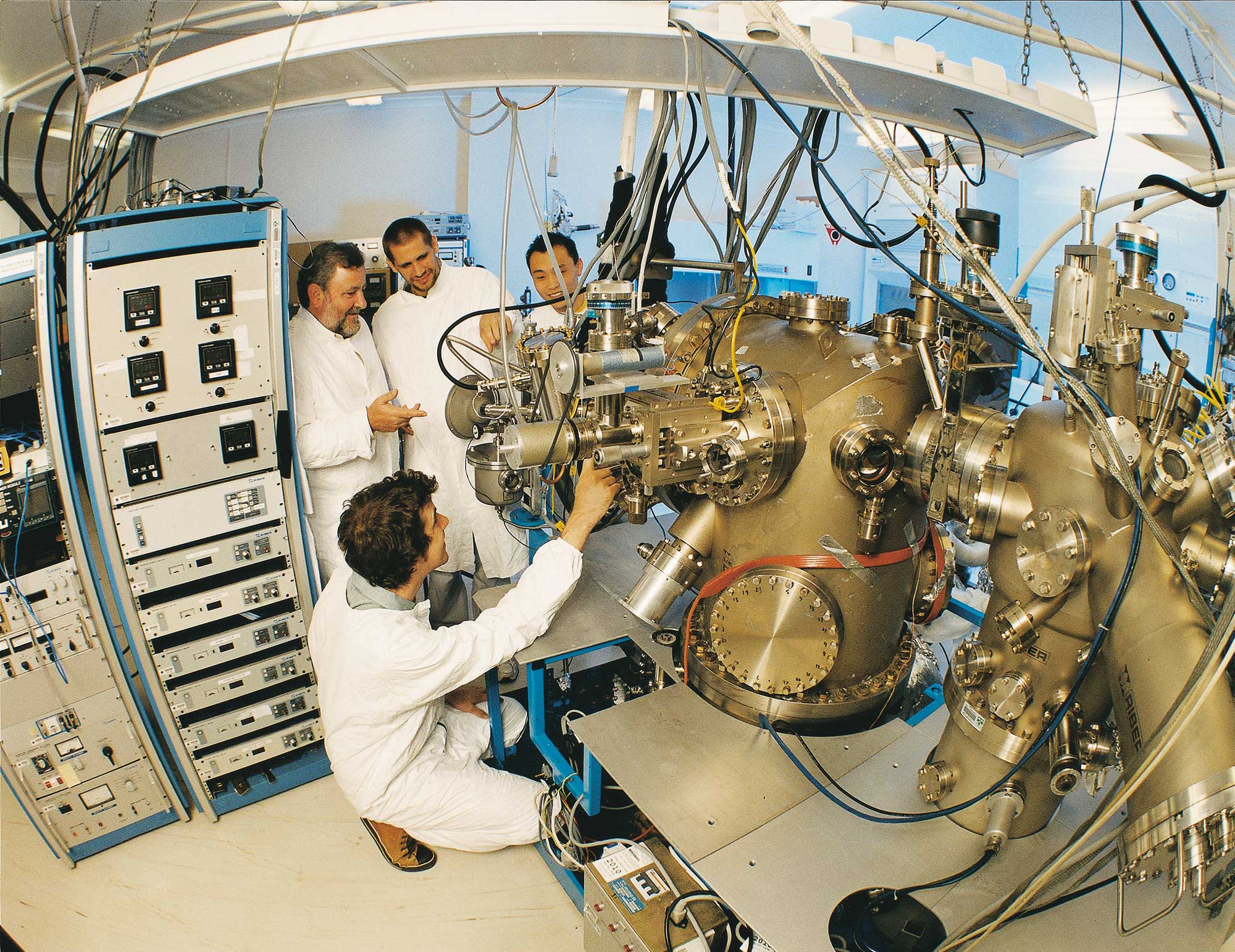
Atomic force microscopy (AFM) is one of the most versatile characterisation methods. AFM performs scanning probe microscopy, scanning the surface of a material with a nanoscale cantilever, either through direct contact or through oscillating the cantilever just above the surface. When the cantilever is positioned in close proximity to the surface, forces between the tip and the sample lead to deflection of the cantilever, which is then measured with a laser signal reflected to a photodiode detector. The properties of the material surface such as topography, mechanical properties and tip-surface interaction forces can then be generated leading to an understanding of the material surface at the nanoscale. AFM has a wide range of applications including nanoscale materials and surface characterisation, electrical materials characterisation, interaction forces and mechanical properties mapping. Bio AFM is useful for pharmaceutical studies, immunology studies, biosensing applications, antibody/antigen binding studies, as well as intra-molecular studies such as protein folding.
List of available equipment
TOOL MAKE AND MODEL
LOCATION
Atomic Force Microscope (AFM), Asylum Research Cypher
ANFF QLD UQ - AIBN
Atomic Force Microscope (AFM), Asylum Research Cypher ES
ANFF MATERIALS Newcastle
Atomic Force Microscope (AFM), Asylum Research MFP3D-BIO
ANFF VIC Latrobe
Atomic Force Microscope (AFM), Asylum Research MFP3D-SA
ANFF VIC Latrobe
Atomic Force Microscope (AFM), Bio NanoWizard
ANFF VIC MCN
Atomic Force Microscope (AFM), Bruker Dimension Edge
ANFF NSW UNSW
Atomic Force Microscope (AFM), Bruker Dimension Icon PFTUNA
ANFF VIC MCN
Atomic Force Microscope (AFM), Bruker Dimension Icon XR
ANFF QLD UQ - AIBN
Atomic Force Microscope (AFM), Bruker Icon
ANFF NSW USYD
Atomic Force Microscope (AFM), Bruker MultiMode 8
ANFF SA
Atomic Force Microscope (AFM), Cypher
ANFF VIC Uni Melbourne
Atomic Force Microscope (AFM), Digital Instruments DI3000
ANFF NSW UNSW
Atomic Force Microscope (AFM), Dimension Icon
ANFF VIC MCN
Atomic Force Microscope (AFM), JPK NanoWizard 4XP
ANFF QLD UQ - AIBN
Atomic Force Microscope (AFM), MFP3D
ANFF VIC Uni Melbourne
Atomic Force Microscope (AFM), Nanosurf CoreAFM
ANFF ACT
Atomic Force Microscope (AFM), Park Systems NX20
ANFF QLD Griffith
Raman Spectroscopy System, Horiba / Nanonics XploRA / MultiView 4000
ANFF SA Flinders
TOOL MAKE AND MODEL
LOCATION
Atomic Force Microscope (AFM), Asylum Research Cypher
Atomic force microscope (AFM) with high resolution m
Description
A purpose built AFM in a dedicated enclosure to investigate surface nanomechanics and topography. Modes available: Kelvin probe force microscopy (KPFM); high voltage piezoresponse force microscopy (HV-PFM); scanning tunnelling microscopy (STM); and AM-FM viscoelastic mapping mode.
Related Information
Substrate size of 15mm diameter. Topological map of 30 µm x 30 µm. Atomic force microscope (AFM) with high resolution m
Tool Contact
anff@uq.edu.au
TOOL MAKE AND MODEL
LOCATION
Atomic Force Microscope (AFM), Asylum Research Cypher ES
Atomic force microscope (AFM) for polymer film analysis
Description
An atomic force microscope which performs very high resolution probing of surfaces. The ES model of the Cypher has an environmental chamber, allowing for the control of temperature and the atmosphere around the sample. Dry and liquid AFM is possible with this system.
Related Information
Typical sample size is maximum 10 mm x 10 mm. Scanning window is maximum 30 μm. Atomic force microscope (AFM) for polymer film analysis
Tool Contact
anff@newcastle.edu.au
TOOL MAKE AND MODEL
LOCATION
Atomic Force Microscope (AFM), Asylum Research MFP3D-BIO
Atomic force microscope (AFM) with inverted optical microscope
Description
General use Atomic Force Microscope (AFM) built on a Nikon inverted microscope base for integrated scanning-probe and optical microscopy. Modes available; Kelvin force probe/adhesion and stiffness maps, conductivity maps and single molecule spectroscopy, viscoelastic mapping, magnetic force mapping.
Related Information
Large substrate size can be handled. Topological map of 90 µm x 90 µm with sub-nanometre resolution in Z. Accessories: closed fluid cell, electrochemistry fluid cell, temperature-controlled fluid exchange, polymer heater. Atomic force microscope (AFM) with inverted optical microscope
Tool Contact
p.pigram@latrobe.edu.au
TOOL MAKE AND MODEL
LOCATION
Atomic Force Microscope (AFM), Asylum Research MFP3D-SA
Atomic force microscope (AFM)
Description
A versatile AFM mounted on an active-damping vibration-isolation table in an acoustic-isolation enclosure to improve resolution.Operating Modes: contact and non-contact (AC) AFM, EFM, MFM, lateral force microscopy (LFM), conductive AFM, KPFM, and nanolithography.
Related Information
90 μm X-Y raster scanningAccessory features: closed fluid cell, electrochemistry fluid cell, temperature-controlled fluid exchange (BioHeater™), and polymer heater. Atomic force microscope (AFM)
Tool Contact
p.pigram@latrobe.edu.au
TOOL MAKE AND MODEL
LOCATION
Atomic Force Microscope (AFM), Bio NanoWizard
Atomic force microscope (AFM) for biological samples
Description
AFM with cell adhesion module, suitable for live cell imaging built on a Nikon inverted microscope base.
Related Information
Large substrate size can be handled. Topological map of 90 µm x 90 µm with sub-nanometre resolution in Z. Atomic force microscope (AFM) for biological samples
Tool Contact
mcn-enquiries@nanomelbourne.com
TOOL MAKE AND MODEL
LOCATION
Atomic Force Microscope (AFM), Bruker Dimension Edge
Description
The Bruker Dimension Edge is a high-performance atomic force microscope (AFM) designed for advanced materials research and nanotechnology applications. It incorporates Bruker's PeakForce Tapping® technology, ensuring high-resolution imaging, low noise, and precise measurements.
Related Information
Tool Contact
anff@unsw.edu.au
TOOL MAKE AND MODEL
LOCATION
Atomic Force Microscope (AFM), Bruker Dimension Icon PFTUNA
Description
The Dimension Icon AFM features a number of application modules such as ScanAsyst, Peak Force QNMTM (PFQNM) and electrical characterisations such as Kelvin Probe Force Microscopy (KPFM), Scanning Capacitance Microscopy (SCM), Tunneling Current AFM (TUNA), and Piezo Response Force Microscopy (PFM). KPFM measures material work function as well as surface charge. SCM is one of the primary techniques for doping profile mapping in semiconductor industry. PeakForce TUNA is an ideal method for probing conductivity of fragile samples such as organic photovoltaics, conductive nanotubes, and nanoparticles. PFTUNA provides direct, precise force control and eliminates lateral forces. TUNA can measure material’s electrical conductivity with wide range of current from fA-uA. PFM enables high-resolution nanoscale characterisation of piezoresponsive materials and topographical imaging using Contact Mode scanning.
Related Information
Peak Force TUNA is an ideal method for probing conductivity of fragile samples such as organic photovoltaics, conductive nanotubes, and nanoparticles. It overcomes the limitations of traditional contact-mode-based conductive AFM techniques, which are severely restricted by sample damage or probe tip contamination from CAFM lateral forces. PeakForce TUNA provides direct, precise force control and eliminates lateral forces. This enables routine highsensitivity and high-resolution current imaging.
Tool Contact
mcn-enquiries@nanomelbourne.com
TOOL MAKE AND MODEL
LOCATION
Atomic Force Microscope (AFM), Bruker Dimension Icon XR
Description
Modes available: PeakForce Tapping, Kevlvin Probe Force Microscopy, TUNA, PeakForce Quantitative Nanomechanical Mapping.
Related Information
Tool Contact
anff@uq.edu.au
TOOL MAKE AND MODEL
LOCATION
Atomic Force Microscope (AFM), Bruker MultiMode 8
AFM Microscope
Description
The Bruker MultiMode 8 is an advanced atomic force microscope (AFM) designed for high-resolution imaging and nanomechanical analysis. It combines PeakForce Tapping® technology with Quantitative Nanomechanical Mapping (QNM) to provide detailed insights into surface properties, elasticity, adhesion, and deformation.
Related Information
Very high-resolution type of Scanning probe microscope AFM Microscope
Tool Contact
anff-sa@adelaide.edu.au
TOOL MAKE AND MODEL
LOCATION
Atomic Force Microscope (AFM), Cypher
Environmental Control & Blue Drive; Piezo Force Microscopy, Mechanical & Electrical properties investigations
Description
AFM with Blue Drive and Environmental control
Related Information
Travel: X, Y=30um, Z=7um Environmental Control & Blue Drive; Piezo Force Microscopy, Mechanical & Electrical properties investigations
Tool Contact
elena.taran@unimelb.edu.au
TOOL MAKE AND MODEL
LOCATION
Atomic Force Microscope (AFM), Digital Instruments DI3000
Atomic force microscope (AFM)
Description
Atomic Force Microscope DI-3000 provides an ability to image and analyse surface topography of conducting and dielectric films as well as adsorbed molecules and nanoparticles by a variety of high resolution surface imaging techniques.
Related Information
More information to come. Atomic force microscope (AFM)
Tool Contact
anff@unsw.edu.au
TOOL MAKE AND MODEL
LOCATION
Atomic Force Microscope (AFM), Dimension Icon
Atomic force microscope (AFM) with various condition control and usability modules
Description
The Dimension Icon AFM features a number of application modules such as ScanAsyst, Peak Force QNMTM (PFQNM), electrical characterisation and heating and cooling studies. The ScanAsyst imaging mode performs automatic image optimisation by controlling the tip-sample interaction force for faster and more consistent imaging results. The PFQNM mode analyses tip-sample interaction forces and generates quantitative nanoscale maps of mechanical properties, including modulus, adhesion, deformation, and dissipation. PFQNM operates over an extremely wide range to characterise a large variety of sample types. The AFM executes temperature control and thermal analysis on samples from -35°C to 250°C while scanning in various AFM modes.
Related Information
Features a large sample platform. Atomic force microscope (AFM) with various condition control and usability modules
Tool Contact
mcn-enquiries@nanomelbourne.com
TOOL MAKE AND MODEL
LOCATION
Atomic Force Microscope (AFM), JPK NanoWizard 4XP
Atomic force microscope (AFM) for biological samples
Description
AFM with cell adhesion module, suitable for live cell imaging built on a Zeiss inverted microscope base. Modes available: fluid cell; temperature and gas control for biological samples; cohesion module (piezo crystal 100 µm in Z); optical/AFM image overlay; and electrochemical unit.
Related Information
Large substrate size can be handled. Topological map of 90 µm x 90 µm with sub-nanometre resolution in Z. Atomic force microscope (AFM) for biological samples
Tool Contact
anff@uq.edu.au
TOOL MAKE AND MODEL
LOCATION
Atomic Force Microscope (AFM), MFP3D
AFM integrated with a inverted microscope and a camera for top and bottom views
Description
AFM integrated with optical microscopy
Related Information
Travel: X, Y=90um, Z=14um AFM integrated with a inverted microscope and a camera for top and bottom views
Tool Contact
elena.taran@unimelb.edu.au
TOOL MAKE AND MODEL
LOCATION
Atomic Force Microscope (AFM), Nanosurf CoreAFM
Atomic Force Microscope (AFM)
Description
The Nanosurf AFM provides access to static force, lateral force, standard spectroscopy, standard lithography, dynamic force, phase Contrast, force Modulation or magnetic force, as well as optional extras such as a lithography and conductive AFM mode.
Related Information
The systems key parameters for sample size: diameter 100 mm, max,. sample height 10 mm and a scan range of XYZ: 100 μm x 100 μm x 12 μm).
Tool Contact
horst.punzmann@anu.edu.au
TOOL MAKE AND MODEL
LOCATION
Raman Spectroscopy System, Horiba / Nanonics XploRA / MultiView 4000
Raman confocal microscope and atomic force microscope (AFM) with tip-enhanced Raman spectroscopy (TERS) capability
Description
Raman spectroscopy system, including a confocal microscope and an atomic force microscope which can perform tip enhanced Raman spectroscopy (TERS)
Related Information
Confocal Raman system with large area scanning stage. Lasers available are 532, 638 and 786nm. TERS option allows spectra to be recorded with a spatial resolution of 90nm. Raman confocal microscope and atomic force microscope (AFM) with tip-enhanced Raman spectroscopy (TERS) capability
Tool Contact
Jason.Gascooke@flinders.edu.au