
Atomic Layer Deposition (ALD)
Atomic Layer Deposition (ALD)
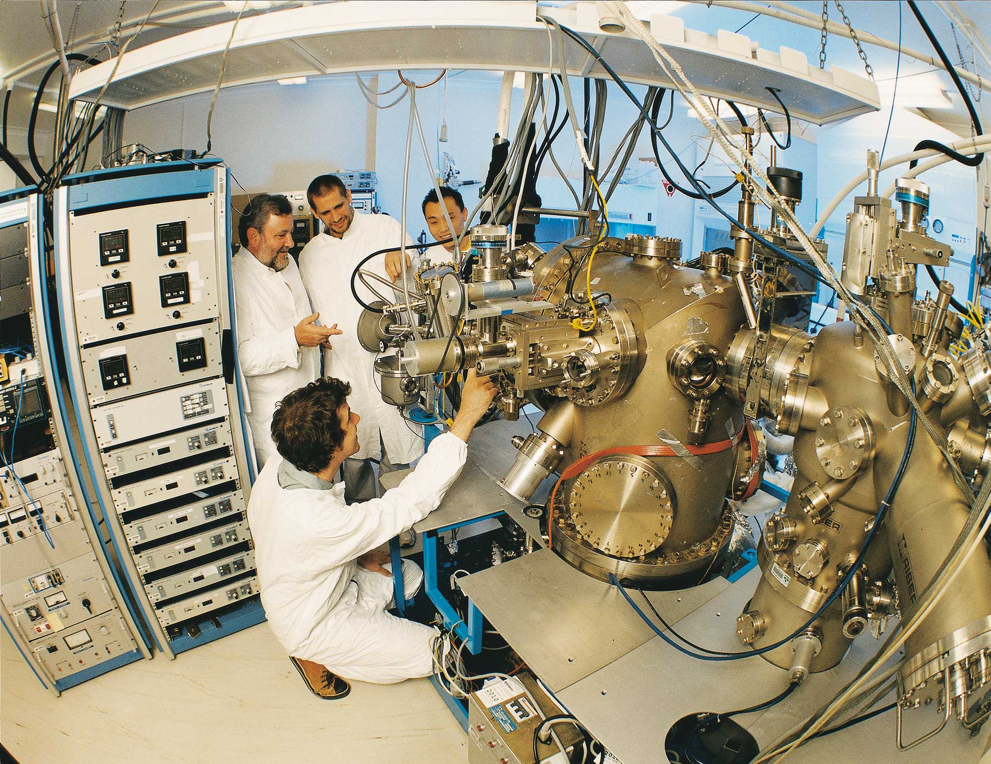
Atomic Layer Deposition (ALD) involves the deposition of materials one atomic monolayer at a time. It forms extremely uniform, conformal, pin-hole-free coatings even on high-aspect-ratio structures. This is achieved by pulsing a chemical precursor onto a hydroxylated substrate surface which reacts, resulting in a monolayer of material to be formed. The unused precursor is purged from the chamber and then the surface is again hydroxylated with water vapour or oxygen, followed by another purge. These steps are then repeated until the desired thickness of material is achieved. ALD has a vast array of applications from semiconductors, MEMS, nanostructures and optics through to wear-resistant coatings.
List of available equipment
TOOL MAKE AND MODEL
LOCATION
Amotic Layer Deposition (ALD) system
ANFF SA Flinders
Amotic Layer Deposition (ALD) system, Cambridge NanoTech Fiji 200
ANFF VIC MCN
Amotic Layer Deposition (ALD) system, Cambridge NanoTech Savannah S100
ANFF VIC MCN
Amotic Layer Deposition (ALD) system, Cambridge NanoTech Savannah S200
ANFF NSW UNSW
Amotic Layer Deposition (ALD) system, PicoSun R-200
ANFF NSW UNSW
Atomic layer deposition(ALD), Picosun R200
ANFF NSW USYD
Atomic Layer Deposition (ALD) system, Picosun R-200 advanced
ANFF QLD UQ - AIBN
TOOL MAKE AND MODEL
LOCATION
Amotic Layer Deposition (ALD) system
Atomic Layer Deposition System
Description
The Atomic Layer Deposition (ALD) system designed for high-precision thin film deposition on wafers, 3D objects, and nanoparticles. It is widely used in semiconductor research, MEMS fabrication, and optical coatings.
Related Information
Configurable ALD system. Atomic Layer Deposition System
Tool Contact
Jason.Gascooke@flinders.edu.au
TOOL MAKE AND MODEL
LOCATION
Amotic Layer Deposition (ALD) system, Cambridge NanoTech Fiji 200
Plasma assisted atomic layer deposition (PA-ALD) System
Description
The Fiji F200 is capable of both thermal and Plasma Assisted ALD (PA-ALD). PA-ALD expands the window for materials by decreasing activation energy and allows for deposition at lower temperatures to reduce precursor decomposition, deposition times and film contaminations. This tool is equipped to enable Cambridge Nanotech’s unique Exposure Mode™ for thin film deposition on ultra high aspect ratio substrates. In-situ film growth can be monitored using a spectroscopic ellipsometry.
Related Information
Substrate size - Up to 6 inch diameter. Maximum substrate heating - 500°C. Available ALD films- Al2O3, TiO2, SiO2, SnO2, ZnO, Ta2O5, MoO3, HfO2, TiN, AZO. Plasma assisted atomic layer deposition (PA-ALD) System
Tool Contact
mcn-enquiries@nanomelbourne.com
TOOL MAKE AND MODEL
LOCATION
Amotic Layer Deposition (ALD) system, Cambridge NanoTech Savannah S100
Atomic layer deposition (ALD) system in a glovebox
Description
This glovebox-integrated thermal ALD system allows the user to deposit materials in controlled environments.
Related Information
Available films- Al2O3, TiO2, WO3, NiOx. Compatible up to 4 inch diameter sample size Atomic layer deposition (ALD) system in a glovebox
Tool Contact
mcn-enquiries@nanomelbourne.com
TOOL MAKE AND MODEL
LOCATION
Amotic Layer Deposition (ALD) system, Cambridge NanoTech Savannah S200
Atomic layer deposition (ALD) system with two precursor sources
Description
ALD system, two precursor sources
Related Information
More information to come. Atomic layer deposition (ALD) system with two precursor sources
Tool Contact
anff@unsw.edu.au
TOOL MAKE AND MODEL
LOCATION
Amotic Layer Deposition (ALD) system, PicoSun R-200
Small Chip to 200mm substrate size temp range 100-500 degC. Setup for deposition Al2O3 and HfO2
Description
The Picosun R-200 is an advanced Atomic Layer Deposition (ALD) system designed for high-precision thin film deposition on wafers, 3D objects, and nanoparticles. It is widely used in semiconductor research, MEMS fabrication, and optical coatings.
Related Information
Small Chip to 200mm substrate size temp range 100-500 degC. Setup for deposition Al2O3 and HfO2
Tool Contact
anff@unsw.edu.au
TOOL MAKE AND MODEL
LOCATION
Atomic Layer Deposition (ALD) system, Picosun R-200 advanced
Description
The Picosun R-200 is an advanced Atomic Layer Deposition (ALD) system designed for high-precision thin film deposition on wafers, 3D objects, and nanoparticles. It is widely used in semiconductor research, MEMS fabrication, and optical coatings.
Related Information
Tool Contact
anff@uq.edu.au