Focused Ion Beam (FIB) milling
Focused Ion Beam (FIB) milling
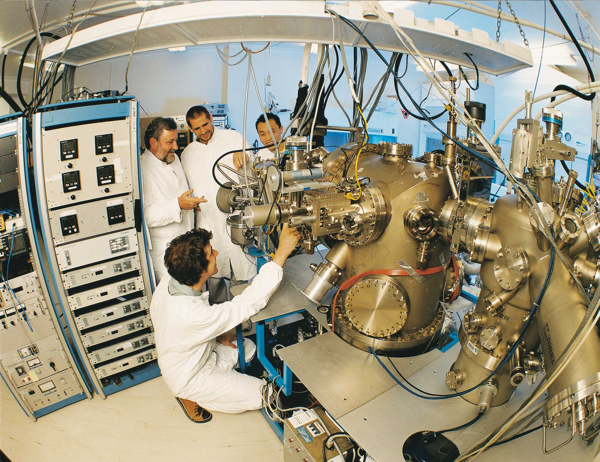
Focused Ion Beam (FIB) milling provides significant advantages as a single-step, nanoscale prototyping method that doesn’t require a mask or resist. It is capable of performing: subtractive lithography in which atoms are locally milled away by physical sputtering with sub-10nm resolution; additive lithography in which materials are locally deposited with sub-10nm resolution; local ion implantation for fabrication of an etching mask for subsequent pattern transfer; and direct material modification by ion-induced mixing. FIB milling is a versatile technique with a wide range of applications including advanced materials development/characterisation; resist-free, high-resolution patterning of nanostructures; cross-sectional analysis of samples; sample preparation for transmission electron microscopy (TEM) and for atom probe analysis.
List of available equipment
TOOL MAKE AND MODEL
LOCATION
FIB-SEM, FEI Helios NanoLab 600 Dual Beam
ANFF VIC MCN
FIB-SEM, Zeiss Crossbeam 550XL
ANFF NSW USYD
TOOL MAKE AND MODEL
LOCATION
FIB-SEM, FEI Helios NanoLab 600 Dual Beam
Scanning electron microscope with focused ion beam for milling (FIB-SEM)
Description
Ultra-high resolution three dimensional imaging for topography, surface morphology and maskless ion beam direct lithography.
Related Information
Ultra-high resolution imaging of samples of all sizes up to 6-inch wafers. The 5-axis stage and 100mm stage movement add flexibility to this equipment. Choice of Secondary Electrons (SE) detector best for topography images and Back-Scattered Electrons (BSE) detector for studies of features deep beneath the surface. Ion beam patterning with 30 kV accelerating voltage and variable currents. Scanning electron microscope with focused ion beam for milling (FIB-SEM)
Tool Contact
mcn-enquiries@nanomelbourne.com