
Plasma Enhanced Chemical Vapour Deposition (PECVD)
Plasma Enhanced Chemical Vapour Deposition (PECVD)
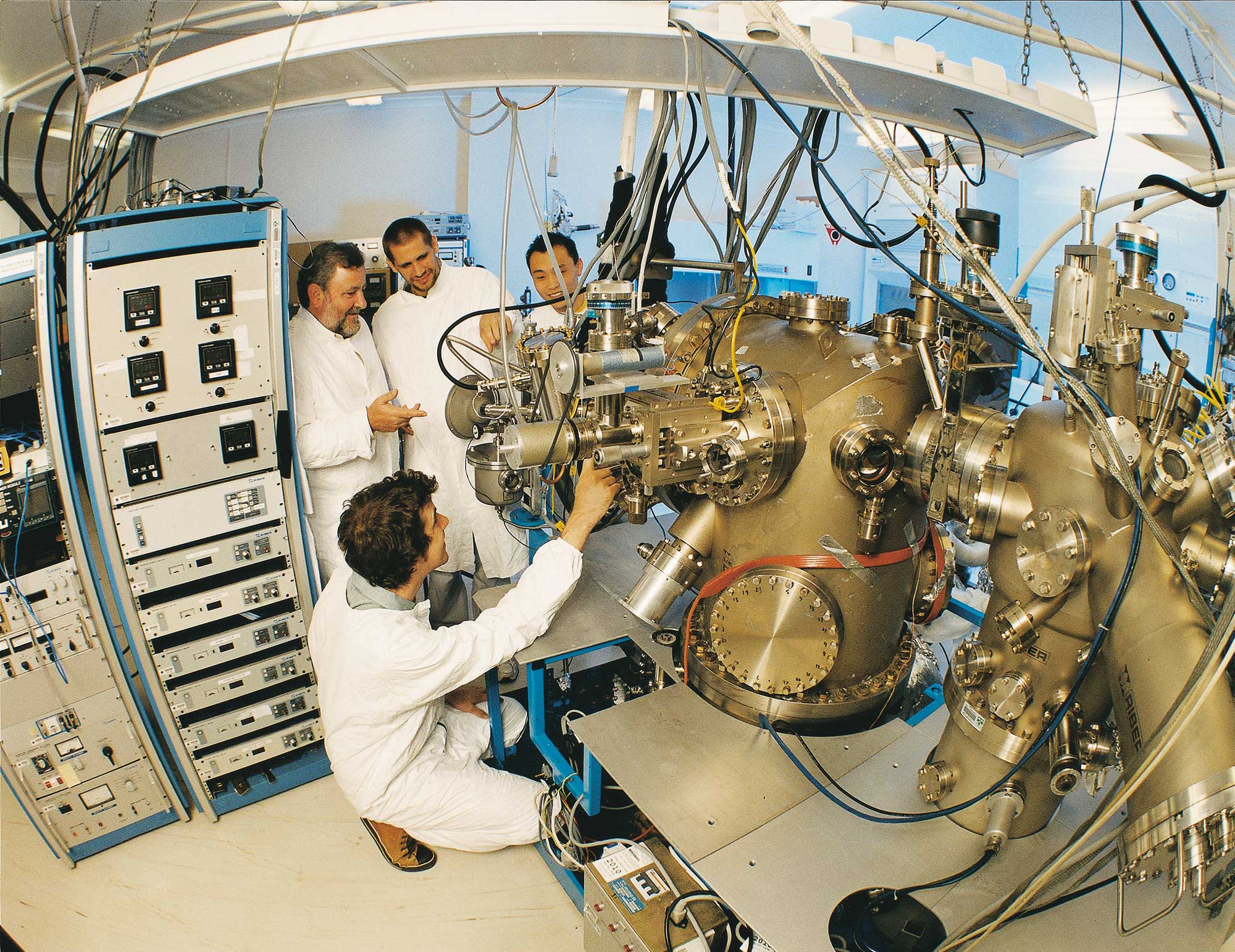
Plasma Enhanced Chemical Vapour Deposition (PECVD) uses a plasma to deposit a thin film of silicon dioxide or silicon nitrate onto a substrate. PECVD uses lower temperatures than the furnace systems to achieve an insulating layer on a variety of materials. PECVD is used in optics, microelectronics, energy applications, packaging and chemistry for the deposition of anti-reflective coatings, scratch resistant transparent coatings, electronically active layers, passivation layers, dielectric layers, isolating layers, etch stop layers, encapsulation and chemical protective coatings.
List of available equipment
TOOL MAKE AND MODEL
KEY DIFFERENTIATOR
LOCATION
Chemical Vapour Deposition- Atomate
Chemical vapour deposition (CVD) system for carbon nanotube and graphene growth
Materials Node
University of Newcastle
Description
Chemical Vapour Deposition specifically to fabricate materials such as carbon nanotubes or graphene by exposing a substrate to reactive precursors.
Related Information
Furnace tube has an inner diameter of 50 μm.
Tool Contact
anff@newcastle.edu.au
Furnace- Labec / MKS HTF40/12 / Various
Tube furnace and chemical vapour deposition system (CVD)
Flinders University
SA Node
Description
High temperature furnace with a programmable gas flow system.
Related Information
Up to 1,200°C quartz tube furnace attached to a programmable 4 channel gas flow manifold suitable for chemical vapour deposition.
Tool Contact
ANFF-SA@unisa.edu.au
Inductively coupled plama chemical vapour deposition (ICPCVD)- Oxford Instruments Plasmalab80 plus
System for ICP plasma deposition
University of Western Australia
WA Node
Description
Thin film deposition via Inductively Coupled Plasma Enhanced Chemical Vapour Deposition (ICPCVD)
Related Information
Process gases: SiH4, NH3, N2O, O2/CF4. Typical deposited materials: Si, SiOx, SiNx, and certain other materials upon request.
Tool Contact
anff-wa@uwa.edu.au
Oxford Instruments Plasmalab 100 – PECVD setup
Plasma enhanced chemical vapour deposition system (PECVD)
NSW Node
University of New South Wales
Description
PECVD
Related Information
More information to come.
Tool Contact
anff@unsw.edu.au
Oxford Instruments Plasmalab 100
Plasma enhanced chemical vapour deposition system (PECVD) for depositing SiOx, SiNx, a-Si
ACT Node
Australian National University (ANU)
Description
Deposit dielectrics SiOx, SiNx and amorphous Si
Related Information
Maximum electrode/sample temperature 650°C
Tool Contact
horst.punzmann@anu.edu.au
Oxford Instruments PlasmaPro ICP – PECVD
Plasma enhanced chemical vapour deposition system (PECVD) for depositing SiOx and SiN
Melbourne Centre for Nanofabrication
VIC Node
Description
Offers fast, affordable deposition at relatively low temperatures.
Related Information
Deposits SiO2, Si3N4, and amorphous Silicon at 100-400 degrees C.
Tool Contact
mcn-enquiries@nanomelbourne.com
PECVD Oxford PlasmaLab
More information to come.
Melbourne Centre for Nanofabrication
VIC Node
Description
Used to coat planar samples with Silicon Oxide or Silicon Nitride thin film
Related Information
More information to come.
Tool Contact
mcn-enquiries@nanomelbourne.com
Plasma Polymerisation Reactors
Deposition of a variety of organic films, including dedicated reactors for air plasma, allylamine (-NH2), acrylic acid (-COOH) and octadiene (-CH2). Samples up to 20 cm in diameter
Swinburne University of Technology
VIC Node
Description
Custom built reactors to deposit a wide variety of organic thin films via plasma enhanced chemical vapour deposition (PE-CVD)
Related Information
More information to come.
Tool Contact
kljarvis@swin.edu.au
Sentech SI 500D ICPCVD
System for ICP plasma deposition
University of Western Australia
WA Node
Description
Thin film deposition via Inductively Coupled Plasma Enhanced Chemical Vapour Deposition (ICPCVD). Variable plasma properties providing high density, low ion energy, and low pressure plasma deposition of dielectric films. A large variety of substrates from wafers up to 200 mm diameter to parts loaded on carriers can be processed.
Related Information
Gases: NH3, N2O, SiH4, O2, H2, O2/CF4 etc. Typical deposited materials: Si, SiOx, SiNx, and certain other materials upon request.
Tool Contact
anff-wa@uwa.edu.au
TOOL MAKE AND MODEL
KEY DIFFERENTIATOR
LOCATION
Chemical Vapour Deposition- Atomate
Chemical vapour deposition (CVD) system for carbon nanotube and graphene growth
Materials Node
University of Newcastle
Description
Chemical Vapour Deposition specifically to fabricate materials such as carbon nanotubes or graphene by exposing a substrate to reactive precursors.
Related Information
Furnace tube has an inner diameter of 50 μm.
Tool Contact
anff@newcastle.edu.au
TOOL MAKE AND MODEL
KEY DIFFERENTIATOR
LOCATION
Furnace- Labec / MKS HTF40/12 / Various
Tube furnace and chemical vapour deposition system (CVD)
Flinders University
SA Node
Description
High temperature furnace with a programmable gas flow system.
Related Information
Up to 1,200°C quartz tube furnace attached to a programmable 4 channel gas flow manifold suitable for chemical vapour deposition.
Tool Contact
ANFF-SA@unisa.edu.au
TOOL MAKE AND MODEL
KEY DIFFERENTIATOR
LOCATION
Inductively coupled plama chemical vapour deposition (ICPCVD)- Oxford Instruments Plasmalab80 plus
System for ICP plasma deposition
University of Western Australia
WA Node
Description
Thin film deposition via Inductively Coupled Plasma Enhanced Chemical Vapour Deposition (ICPCVD)
Related Information
Process gases: SiH4, NH3, N2O, O2/CF4. Typical deposited materials: Si, SiOx, SiNx, and certain other materials upon request.
Tool Contact
anff-wa@uwa.edu.au
TOOL MAKE AND MODEL
KEY DIFFERENTIATOR
LOCATION
Oxford Instruments Plasmalab 100 – PECVD setup
Plasma enhanced chemical vapour deposition system (PECVD)
NSW Node
University of New South Wales
Description
PECVD
Related Information
More information to come.
Tool Contact
anff@unsw.edu.au
TOOL MAKE AND MODEL
KEY DIFFERENTIATOR
LOCATION
Oxford Instruments Plasmalab 100
Plasma enhanced chemical vapour deposition system (PECVD) for depositing SiOx, SiNx, a-Si
ACT Node
Australian National University (ANU)
Description
Deposit dielectrics SiOx, SiNx and amorphous Si
Related Information
Maximum electrode/sample temperature 650°C
Tool Contact
horst.punzmann@anu.edu.au
TOOL MAKE AND MODEL
KEY DIFFERENTIATOR
LOCATION
Oxford Instruments PlasmaPro ICP – PECVD
Plasma enhanced chemical vapour deposition system (PECVD) for depositing SiOx and SiN
Melbourne Centre for Nanofabrication
VIC Node
Description
Offers fast, affordable deposition at relatively low temperatures.
Related Information
Deposits SiO2, Si3N4, and amorphous Silicon at 100-400 degrees C.
Tool Contact
mcn-enquiries@nanomelbourne.com
TOOL MAKE AND MODEL
KEY DIFFERENTIATOR
LOCATION
PECVD Oxford PlasmaLab
More information to come.
Melbourne Centre for Nanofabrication
VIC Node
Description
Used to coat planar samples with Silicon Oxide or Silicon Nitride thin film
Related Information
More information to come.
Tool Contact
mcn-enquiries@nanomelbourne.com
TOOL MAKE AND MODEL
KEY DIFFERENTIATOR
LOCATION
Plasma Polymerisation Reactors
Deposition of a variety of organic films, including dedicated reactors for air plasma, allylamine (-NH2), acrylic acid (-COOH) and octadiene (-CH2). Samples up to 20 cm in diameter
Swinburne University of Technology
VIC Node
Description
Custom built reactors to deposit a wide variety of organic thin films via plasma enhanced chemical vapour deposition (PE-CVD)
Related Information
More information to come.
Tool Contact
kljarvis@swin.edu.au
TOOL MAKE AND MODEL
KEY DIFFERENTIATOR
LOCATION
Sentech SI 500D ICPCVD
System for ICP plasma deposition
University of Western Australia
WA Node
Description
Thin film deposition via Inductively Coupled Plasma Enhanced Chemical Vapour Deposition (ICPCVD). Variable plasma properties providing high density, low ion energy, and low pressure plasma deposition of dielectric films. A large variety of substrates from wafers up to 200 mm diameter to parts loaded on carriers can be processed.
Related Information
Gases: NH3, N2O, SiH4, O2, H2, O2/CF4 etc. Typical deposited materials: Si, SiOx, SiNx, and certain other materials upon request.
Tool Contact
anff-wa@uwa.edu.au