
Thermal Scanning Probe Lithography (t-SPL)
Thermal Scanning Probe Lithography (t-SPL)
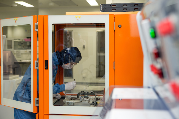
Thermal Scanning Probe Lithography (t-SPL) is a 3D direct-write lithography technique that provides sub-10nm resolution with sub-2nm vertical accuracy in ambient conditions. A 1,000°C cantilevered tip sublimates PPA resist as it scans over a sample, before the tip quickly cools to provide real-time topological AFM-type characterisation. The process isn’t reliant on an ion gun or electron beam (helpful when processing sensitive materials); it operates at ambient temperature, pressure, low voltage, and under N2 atmosphere instead of requiring a specialist environment. The ease of use and high resolution means it is ideal for rapid fabrication of three-dimensional nanostructures including the fabrication of novel devices and components for nanophotonics, nanooptics, nanoelectronics, and plasmonics applications.
List of available equipment
TOOL MAKE AND MODEL
KEY DIFFERENTIATOR
LOCATION
Thermal Scanning Probe Lithography-NanoFrazor
Thermal Scanning Probe Lithography (t-SPL) system
Melbourne Centre for Nanofabrication
VIC Node
Description
Operates at ambient temperature, pressure, low voltage, and under N2 atmosphere.Not reliant on ion gun or electron beam which is good when processing sensitive materials and devices.
Related Information
Uses a 1,000°C cantilever tip to sublimate PPA resist.Sub -10nm resolution, <2nm vertical accuracy
Tool Contact
mcn-enquiries@nanomelbourne.com