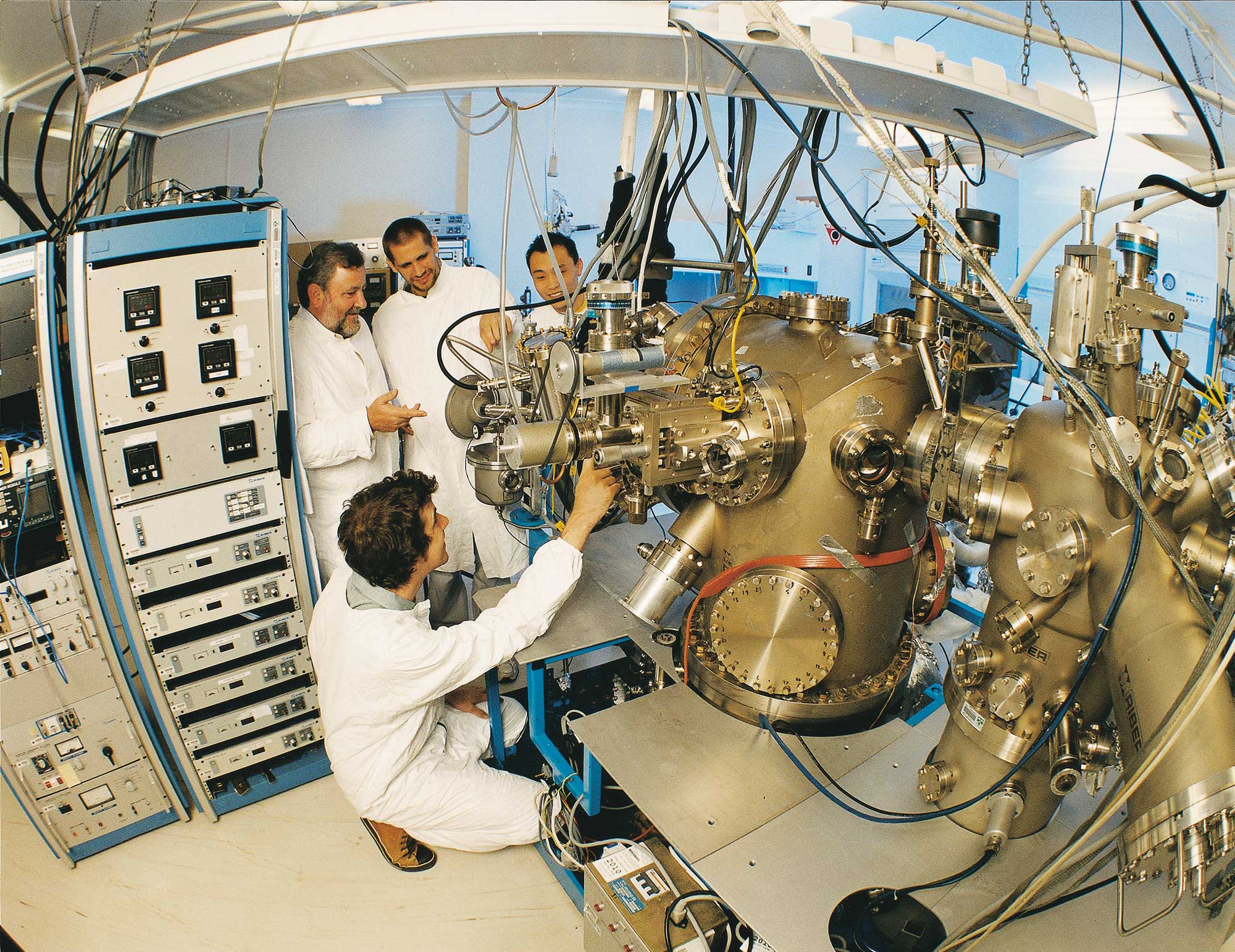
Wafer Bonding
Wafer Bonding
Bonding a wafer to another wafer is a step commonly used when packaging components in an micro or nanoelectrical device. It can help a form new functions in a device, or can ensure mechanical and hermetic encapsulation of devices and electronics. The result is irreversible. Common bonding methods include using heat or with an adhesive for thermally sensitive samples.

List of available equipment
TOOL MAKE AND MODEL
LOCATION
Die bonder, TPT HB75
ANFF NSW USYD
Flip Chip Bonder, Finetech Fineplacer-96
ANFF WA
Flip chip bonder, Finetech Fineplacer lambda
ANFF NSW USYD
Flip Chip Bonder, Finetech Fineplacer Lambda
ANFF ACT
Reflow Solder Oven, UniTemp RVS-210
ANFF WA
Substrate Bonder, EVG520
ANFF SA
Wafer bonder, EVG501
ANFF NSW USYD
TOOL MAKE AND MODEL
LOCATION
Flip Chip Bonder, Finetech Fineplacer-96
Flip chip bonder
Description
Manual flip-chip bonder for small substrates below 5x5mm2
Related Information
Max. die/package size: 16 mm (pick-n-place only). Min. die/package size: 5 mm × 5 mm. Substrate size: 20 mm × 20 mm (thermal compression). Bonding mechanism: thermo-compression (bonding force 0.1 ~ 200 N). Reflow (RT ~ 400 °C, heating rate: 20 °C/s) Flip chip bonder
Tool Contact
anff-wa@uwa.edu.au
TOOL MAKE AND MODEL
LOCATION
Flip chip bonder, Finetech Fineplacer lambda
Sub-Micron Die Bonder
Description
Sub-micron die-bonder for precision die attach and advanced chip packaging.
Related Information
Ultrasonic or thermosonic bonding, formic acid, adhesive dispense module. Sub-Micron Die Bonder
Tool Contact
rpf.queries@sydney.edu.au
TOOL MAKE AND MODEL
LOCATION
Flip Chip Bonder, Finetech Fineplacer Lambda
Flip chip bonder
Description
Used to align and place/bond chips on PCB or larger chips using metal bonding.
Related Information
0.5 micron placement accuracy. Substrate temperature 400 degrees C. Thermocompression bonding. Flip chip bonder
Tool Contact
horst.punzmann@anu.edu.au
TOOL MAKE AND MODEL
LOCATION
Reflow Solder Oven, UniTemp RVS-210
Reflow solder oven
Description
The UniTemp RVS-210 is a compact reflow solder system designed for laboratory and cleanroom applications, specifically for reflowing indium bumps into balls for flip-chip bonding. It features a vacuum-sealed chamber with a viewing window, ensuring precise visual control of the soldering process.
Related Information
Allows reflow of Indium bumps in forming gas atmosphere. Indium is widely used for electrical interconnections in various semiconductor devices due to its physicochemical properties. An indium bump array is most commonly fabricated using a lift-off process in conjunction with photolithography. After indium columns are fabricated, a reflow process is performed to form bumps which are of the same height thus ensuring contact is made uniformly during the bonding process. Reflow solder oven
Tool Contact
anff-wa@uwa.edu.au
TOOL MAKE AND MODEL
LOCATION
Substrate Bonder, EVG520
Substrate bonder
Description
Designed for bonding, embossing and nanoimprinting applications the system can thermally bond glass substrates and emboss channel geometries into substrates.
Related Information
Capable of all wafer bonding processes such as thermo-compression, fusion or low temperature bonding. It is configured to allow hot embossing of polymers and even glass. Substrate bonder
Tool Contact
ANFF-SA@unisa.edu.au
