Porous silicon’s high surface area and versatility make it a game-changer for next-gen sensors and medical devices.
Porous silicon (PS) is a unique form of silicon (Si) that features tiny nanopores within its structure, making it a highly versatile material with broad potential applications. Its compatibility with silicon-based microelectronics positions it as a promising candidate for a range of electrical and optical devices, such as sensors and solar cells.
The tiny holes in the structure increase the active surface area and allow for infiltration of analytes deeper into the film.

This infiltration greatly enhances the sensitivity and efficiency of PS compared to conventional solid silicon, particularly in optical sensors where the analytes can interact with the sensor’s guided light path. Furthermore, PS offers excellent mechanical and thermal properties while remaining cost-effective.
Despite its benefits, PS faces a major challenge: instability over time. After production, PS film surfaces are typically covered with hydrogen, maintaining stability only for a short time in non-reactive environments. Prolonged exposure to air initiates oxidation, leading to surface instability. Over time, PS films and devices made from them become less reliable. This instability is problematic for many uses, so various techniques are being developed to improve the long-term stability of PS films and devices.
One such promising approach is being explored by Jesse Fletcher, a PhD candidate at the University of Western Australia. Fletcher employs a combination of PS and direct laser writing (DLW) to create stable waveguiding regions in PS thin films, designed for photonic applications. Using DLW in a hydrocarbon atmosphere creates carbonised PS, which is a stabilising thin silicon carbide (SiC) layer on the pore surface.
ANFF-WA supports this cutting-edge work by providing the space and equipment to fabricate PS films via electrochemical anodization of Si wafers in hydrofluoric acid, as well as the necessary post processing steps to develop viable devices.
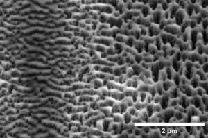
Fletcher’s fabrication method successfully transforms about one-third of the Si wafer’s thickness into PS. The carbonised regions, with their higher refractive index, form a waveguiding core in the PS film, directing and confining light along defined paths. By tuning the optical properties of the PS films, Fletcher produces low-loss materials where propagating light experiences minimal power reduction, especially when compared to solid Si. This low-loss PS enhances the interaction between the optical wave and the material being sensed, resulting in extremely high sensitivities.
Moreover, the ability to create large, on-chip waveguides simplifies the alignment of PS optical sensors with standard, off-the-shelf optical fibres, reducing implementation costs for this emerging technology. This feature makes PS a practical and cost-effective solution for a variety of applications.
The use of PS as a waveguiding platform opens exciting opportunities for highly sensitive sensors in biomedical and environmental monitoring. Its compatibility with biological systems allows organic molecules to stick to it easily. The high surface area also allows functionalisation of the surface, improving the selectivity of the platform for different biomolecules and biomarkers, such as proteins, DNA, metabolites and antibodies. Additionally, by adjusting its porosity, PS can be made bio-inert, bioactive or resorbable, enabling it to safely degrade within the body into orthosilicic acid, a harmless substance.
As stability challenges are overcome, porous silicon has the potential to transform optical and biosensing technologies. Jesse Fletcher’s research on carbonising PS films points toward a future where these ‘silicon sponges’ serve as adaptable, reliable materials for next-generation sensors and devices across numerous industries.
Published 15 October 2024 in ANFF’s 2024 Casebook ‘ANFF NEXT‘
Posted 08 April 2025