Electron Beam Lithography (EBL)
Electron Beam Lithography (EBL)
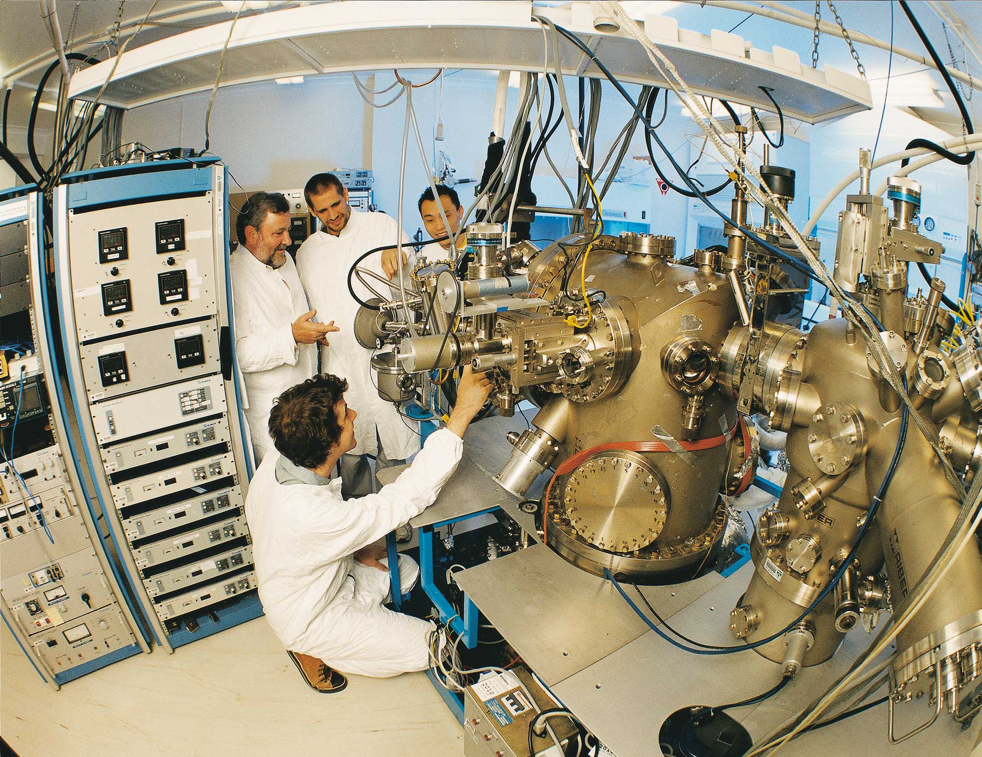
Electron Beam Lithography (EBL) allows users to write patterns with extremely high resolution, smaller than 10nm in size. It makes use of a highly energetic, tightly focused electron beam, which is scanned over a sample coated with an electron-sensitive resist. The electron beam scans the image according to a pattern defined on a CAD file. The sample is then developed in an appropriate solvent which reveals the structures defined into the resist. This acts as a mould for subsequent pattern transfer techniques such as dry etching ormetal lift-off.Due to the high-resolution nature of the technique, EBL has a vast range of applications including nano-electronics, photonics, plasmonics, nano-fluidics, MEMS, x-ray and neutron optics.
List of available equipment
TOOL MAKE AND MODEL
KEY DIFFERENTIATOR
LOCATION
FEI Sirion
Electron beam lithography (EBL) system
NSW Node
University of New South Wales
Description
EBL system, NPGS pattern generator, small write fields
Related Information
More information to come.
Tool Contact
anff@unsw.edu.au
Raith 150
Electron beam lithography (EBL) system
ACT Node
Australian National University (ANU)
Description
Electron-beam lithography tool for sub-µm features, accurate positioning
Related Information
30kV acceleration voltage, fixed beam moving stage, writing field up to 800x800 µm2
Tool Contact
horst.punzmann@anu.edu.au
Vistec EBL 5000
Electron beam lithography (EBL) system
Melbourne Centre for Nanofabrication
VIC Node
Description
EBL that is capable of exposing thick layers of e-beam resist of up to several micrometres with small forward scattering.Fully automated equipment features a laser height measurement for automatic focus adjustment.
Related Information
Can produces ~10nm structures.Metrology functions for self-calibration.Operates at up to 100 keV acceleration voltage.The electron beam spot can be focused to less than 5 nm in diameter. A wide range of beam currents (200 pA – 150 nA) are available for high-throughput as well as high-resolution exposures. 6-inch wafers and mask blanks measuring up to 5 × 5 inches can be processed.Rapid exposure with 50 MHz pattern generator.A laser-guided substrate stage provides 15 nm field stitching error.Maximum writing field of 1 x 1 mm.The overlay accuracy is below 20nm.For the conversion of the CAD patterns into machine specific format, including proximity effect correction (PEC), special software, TRACER and BEAMER from GenIsys GmbH are used.
Tool Contact
mcn-enquiries@nanomelbourne.com
TOOL MAKE AND MODEL
KEY DIFFERENTIATOR
LOCATION
FEI Sirion
Electron beam lithography (EBL) system
Melbourne Centre for Nanofabrication
VIC Node
Description
EBL system, NPGS pattern generator, small write fields
Related Information
More information to come.
Tool Contact
anff@unsw.edu.au
TOOL MAKE AND MODEL
KEY DIFFERENTIATOR
LOCATION
Raith 150
Electron beam lithography (EBL) system
Melbourne Centre for Nanofabrication
VIC Node
Description
Electron-beam lithography tool for sub-µm features, accurate positioning
Related Information
30kV acceleration voltage, fixed beam moving stage, writing field up to 800x800 µm2
Tool Contact
horst.punzmann@anu.edu.au
TOOL MAKE AND MODEL
KEY DIFFERENTIATOR
LOCATION
Vistec EBL 5000
Electron beam lithography (EBL) system
Melbourne Centre for Nanofabrication
VIC Node
Description
EBL that is capable of exposing thick layers of e-beam resist of up to several micrometres with small forward scattering.Fully automated equipment features a laser height measurement for automatic focus adjustment.
Related Information
Can produces ~10nm structures.Metrology functions for self-calibration.Operates at up to 100 keV acceleration voltage.The electron beam spot can be focused to less than 5 nm in diameter. A wide range of beam currents (200 pA – 150 nA) are available for high-throughput as well as high-resolution exposures. 6-inch wafers and mask blanks measuring up to 5 × 5 inches can be processed.Rapid exposure with 50 MHz pattern generator.A laser-guided substrate stage provides 15 nm field stitching error.Maximum writing field of 1 x 1 mm.The overlay accuracy is below 20nm.For the conversion of the CAD patterns into machine specific format, including proximity effect correction (PEC), special software, TRACER and BEAMER from GenIsys GmbH are used.
Tool Contact
mcn-enquiries@nanomelbourne.com