Plasma etching
Home > Equipment > Etching > Plasma etching
Plasma etching

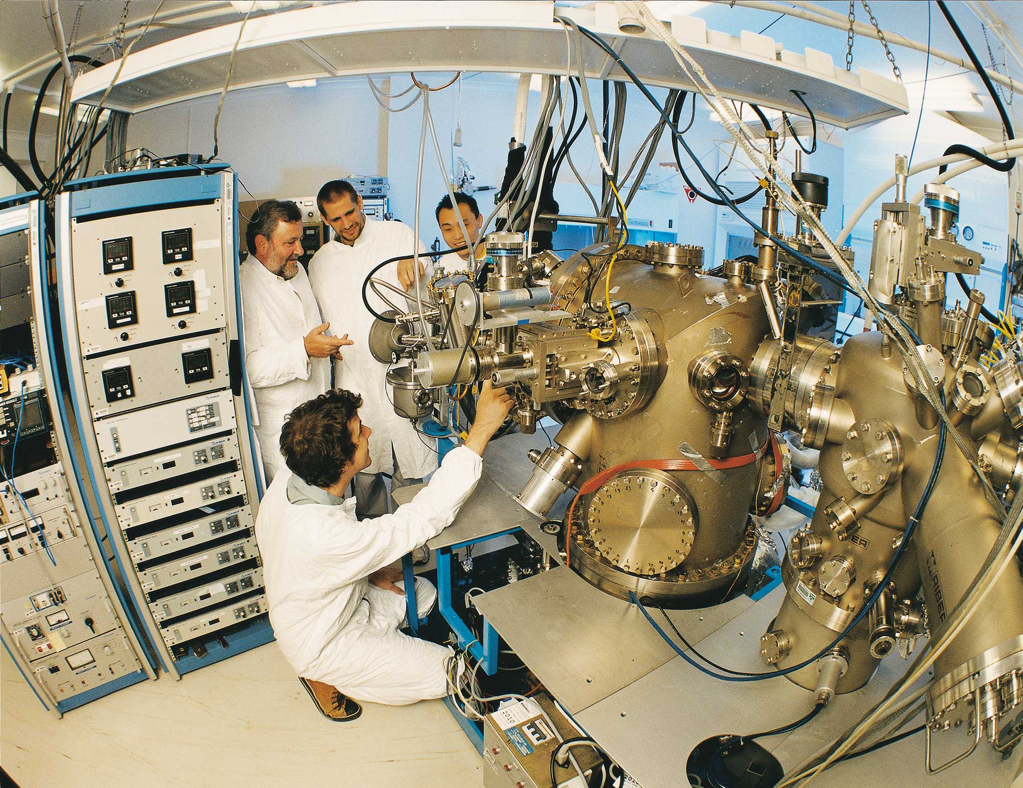
Plasma etching uses a finely controlled plasma to selectively remove material from a substrate.
List of available equipment
TOOL MAKE AND MODEL
KEY DIFFERENTIATOR
LOCATION
Benchtop Plasma Asher
More information to come.
Melbourne Centre for Nanofabrication VIC Node
Description
Harrick plasma etcher / asher
Related Information
More information to come.
Tool Contact
mcn-enquiries@nanomelbourne.com
Cl Etcher
Cl etcher
NSW Node University of Technology Sydney
Description
This high-powered Cl Etcher tool is a top-of-the-line solution for precise material removal tasks, specifically in the semiconductor and integrated circuits industry. It's perfect for creating intricate patternThis high-powered Cl Etcher tool is a top-of-the-line solution for precise material removal tasks, specifically in the semiconductor and integrated circuits industry. It's perfect for creating intricate patterns on silicon wafers, offering up to 1000W of Inductively Coupled Plasma power. What sets this tool apart is its availability of chlorine. The system is specifically designed to be Chlorine compatible, providing a wide range of etching capabilities on various materials. With this tool, you can achieve highly detailed etching at an impressive rate, even on the most complex projects. One of the standout features is its built-in chiller stage. This cooling system ensures your work remains at a controlled temperature throughout the etching process. Not only does this safeguard your silicon wafer from potential heat damage, it also maintains the highest level of precision and consistency in your work. Whether you're new to the world of semiconductor fabrication or a seasoned professional, this Cl Etcher tool brings a new level of reliability and efficiency to your projects. It's designed with usability in mind, so even if you're not entirely sure what your needs are, this tool's versatility and user-friendly features make it a valuable asset for a wide range of tasks.
Related Information
1000w in ICP power, chiller stage
Tool Contact
Toby.Shanley-1@uts.edu.au
Etcher- XeF2
More information to come.
QLD Node University of Queensland
Description
A vapour phase isotropic etching of silicon with very high etch selectivity of silicon to SiO2, SiN, photoresist, and Al.
Related Information
More information to come.
Tool Contact
anff@uq.edu.au
Large Plasma Asher
More information to come.
Melbourne Centre for Nanofabrication VIC Node
Description
General Plasma cleaning system
Related Information
Plasma Asher commonly used to clean materials of organics materials, and can also be used for surface treatment of materials
Tool Contact
mcn-enquiries@nanomelbourne.com
March Instruments PM-600 barrel plasma asher
Barrel benchtop oxygen plasma etcher/asher.
University of Western Australia WA Node
Description
Oxygen plasma etcher/asher.
Related Information
Oxygen plasma etch tool and/or plasma exposure in a barrel electrode configuration.
Tool Contact
anff-wa@uwa.edu.au
Oxford Instruments ICP-100
ICP Etcher, 3KW ICP source, 8 gasses, interferometric etch rate monitor, up to 150mm wafers, ICP etching Chalcogenide,Semiconductor,Photonics materials
Australian National University (ANU) Optofab Node
Description
ICP Etcher, 3KW ICP source, 8 gasses(CHF3,SF6,O2,N2,C4F8,Ar,He) interferometric etch rate monitor, up to 150mm wafers. The Oxford Plasmalab 100 inductively coupled plasma (ICP) etcher is a multipurpose Etching system that provides users anisotropic etching of silicon, silicon oxide, chalcogenide and other dielectric materials. The tool is equipped with a temperature controlled electrode to help users tailor their etch feature profiles. The manual load system can accommodate substrates ranging from 150 mm diameter wafers down to small pieces. Available gases are CH4, CHF3, SF6, C4F8, H2, Ar, and O2 Si based (Si, SiO2& Si3N4), oxides (ITO, TiO2, TeO2, Ta2O5, ZnO, etc), polymers (BCB, SU-8, Polysiloxanes, etc)
Related Information
Dry Etch system,gas available for etching:SF6, CHF3, He, Ar, and O2
Tool Contact
stephen.madden@anu.edu.au
Plasma Cleaner- Tergeo Tabletop
More information to come.
QLD Node University of Queensland
Description
For surface cleaning and surface activation. Used when making a glass-PDMS or PDMS-PDMS microfluidic chip
Related Information
More information to come.
Tool Contact
anff@uq.edu.au
Plasma Etching- LAM Autoetch 480
Plasma Asher
Griffith University QLD Node
Description
Plasma etching of 6 inch wafers using a semi-isotropic dry etch process. Can produce features of 3µm.
Related Information
Utilises SF6 and O. Used to etch SiC, SiN and SiO2 and polymer resists.
Tool Contact
glenn.walker@griffith.edu.au
RIE Etching- South Bay RIE3000
O2 Plasma Asher/RIE
NSW Node University of Sydney
Description
Reactive ion etch system dedicated to O2 and Ar plasma processes
Related Information
Used primarily for resist and sample cleaning.
Tool Contact
rpf.queries@sydney.edu.au
Tepla barrel etcher
Stripping tool
Australian National University (ANU) Optofab Node
Description
The Tepla Barrel Etcher is a versatile high-pressure plasma system designed for efficient cleaning and resist stripping. It excels in removing organic materials and resists with O2-plasma, ensuring clean pattern development with its low power setting. Additionally, it can strip resists and etch SiNx/SiOx layers by incorporating CF4. This robust machine can process either two 4-inch wafers or a single 6-inch wafer simultaneously.
Related Information
Photoresist stripping using O2 and Argon
Tool Contact
stephen.madden@anu.edu.au
TOOL MAKE AND MODEL
KEY DIFFERENTIATOR
LOCATION
Benchtop Plasma Asher
More information to come.
Australian National University (ANU) Optofab Node
Description
Harrick plasma etcher / asher
Related Information
More information to come.
Tool Contact
mcn-enquiries@nanomelbourne.com
TOOL MAKE AND MODEL
KEY DIFFERENTIATOR
LOCATION
Cl Etcher
Cl etcher
Australian National University (ANU) Optofab Node
Description
This high-powered Cl Etcher tool is a top-of-the-line solution for precise material removal tasks, specifically in the semiconductor and integrated circuits industry. It's perfect for creating intricate patternThis high-powered Cl Etcher tool is a top-of-the-line solution for precise material removal tasks, specifically in the semiconductor and integrated circuits industry. It's perfect for creating intricate patterns on silicon wafers, offering up to 1000W of Inductively Coupled Plasma power. What sets this tool apart is its availability of chlorine. The system is specifically designed to be Chlorine compatible, providing a wide range of etching capabilities on various materials. With this tool, you can achieve highly detailed etching at an impressive rate, even on the most complex projects. One of the standout features is its built-in chiller stage. This cooling system ensures your work remains at a controlled temperature throughout the etching process. Not only does this safeguard your silicon wafer from potential heat damage, it also maintains the highest level of precision and consistency in your work. Whether you're new to the world of semiconductor fabrication or a seasoned professional, this Cl Etcher tool brings a new level of reliability and efficiency to your projects. It's designed with usability in mind, so even if you're not entirely sure what your needs are, this tool's versatility and user-friendly features make it a valuable asset for a wide range of tasks.
Related Information
1000w in ICP power, chiller stage
Tool Contact
Toby.Shanley-1@uts.edu.au
TOOL MAKE AND MODEL
KEY DIFFERENTIATOR
LOCATION
Etcher- XeF2
More information to come.
Australian National University (ANU) Optofab Node
Description
A vapour phase isotropic etching of silicon with very high etch selectivity of silicon to SiO2, SiN, photoresist, and Al.
Related Information
More information to come.
Tool Contact
anff@uq.edu.au
TOOL MAKE AND MODEL
KEY DIFFERENTIATOR
LOCATION
Large Plasma Asher
More information to come.
Australian National University (ANU) Optofab Node
Description
General Plasma cleaning system
Related Information
Plasma Asher commonly used to clean materials of organics materials, and can also be used for surface treatment of materials
Tool Contact
mcn-enquiries@nanomelbourne.com
TOOL MAKE AND MODEL
KEY DIFFERENTIATOR
LOCATION
March Instruments PM-600 barrel plasma asher
Barrel benchtop oxygen plasma etcher/asher.
Australian National University (ANU) Optofab Node
Description
Oxygen plasma etcher/asher.
Related Information
Oxygen plasma etch tool and/or plasma exposure in a barrel electrode configuration.
Tool Contact
anff-wa@uwa.edu.au
TOOL MAKE AND MODEL
KEY DIFFERENTIATOR
LOCATION
Oxford Instruments ICP-100
ICP Etcher, 3KW ICP source, 8 gasses, interferometric etch rate monitor, up to 150mm wafers, ICP etching Chalcogenide,Semiconductor,Photonics materials
Australian National University (ANU) Optofab Node
Description
ICP Etcher, 3KW ICP source, 8 gasses(CHF3,SF6,O2,N2,C4F8,Ar,He) interferometric etch rate monitor, up to 150mm wafers. The Oxford Plasmalab 100 inductively coupled plasma (ICP) etcher is a multipurpose Etching system that provides users anisotropic etching of silicon, silicon oxide, chalcogenide and other dielectric materials. The tool is equipped with a temperature controlled electrode to help users tailor their etch feature profiles. The manual load system can accommodate substrates ranging from 150 mm diameter wafers down to small pieces. Available gases are CH4, CHF3, SF6, C4F8, H2, Ar, and O2 Si based (Si, SiO2& Si3N4), oxides (ITO, TiO2, TeO2, Ta2O5, ZnO, etc), polymers (BCB, SU-8, Polysiloxanes, etc)
Related Information
Dry Etch system,gas available for etching:SF6, CHF3, He, Ar, and O2
Tool Contact
stephen.madden@anu.edu.au
TOOL MAKE AND MODEL
KEY DIFFERENTIATOR
LOCATION
Plasma Cleaner- Tergeo Tabletop
More information to come.
Australian National University (ANU) Optofab Node
Description
For surface cleaning and surface activation. Used when making a glass-PDMS or PDMS-PDMS microfluidic chip
Related Information
More information to come.
Tool Contact
anff@uq.edu.au
TOOL MAKE AND MODEL
KEY DIFFERENTIATOR
LOCATION
Plasma Etching- LAM Autoetch 480
Plasma Asher
Australian National University (ANU) Optofab Node
Description
Plasma etching of 6 inch wafers using a semi-isotropic dry etch process. Can produce features of 3µm.
Related Information
Utilises SF6 and O. Used to etch SiC, SiN and SiO2 and polymer resists.
Tool Contact
glenn.walker@griffith.edu.au
TOOL MAKE AND MODEL
KEY DIFFERENTIATOR
LOCATION
RIE Etching- South Bay RIE3000
O2 Plasma Asher/RIE
Australian National University (ANU) Optofab Node
Description
Reactive ion etch system dedicated to O2 and Ar plasma processes
Related Information
Used primarily for resist and sample cleaning.
Tool Contact
rpf.queries@sydney.edu.au
TOOL MAKE AND MODEL
KEY DIFFERENTIATOR
LOCATION
Tepla barrel etcher
Stripping tool
Australian National University (ANU) Optofab Node
Description
The Tepla Barrel Etcher is a versatile high-pressure plasma system designed for efficient cleaning and resist stripping. It excels in removing organic materials and resists with O2-plasma, ensuring clean pattern development with its low power setting. Additionally, it can strip resists and etch SiNx/SiOx layers by incorporating CF4. This robust machine can process either two 4-inch wafers or a single 6-inch wafer simultaneously.
Related Information
Photoresist stripping using O2 and Argon
Tool Contact
stephen.madden@anu.edu.au