The Australian National University researcher Dr Tuomas Haggren’s light-emitting metasurface goes beyond the limits of normal materials to manipulate how nanoscale patterns affect the properties of light.
From Princess Leia of Star Wars begging for Obi-Wan Kenobi’s help to the holodeck adventures in Star Trek, depictions of holograms have evolved from 3D images that we can see to 3D spaces with which we can interact. More recently, ‘holograms’ have allowed us to resurrect dead celebrities who can perform and interact with audiences. Holograms seem to be infiltrating our daily lives.
While the previous examples describe wonderful visual effects, they aren’t actually holograms but rather sophisticated optical illusions based on the projection and reflection of light from glass, mirrors and other surfaces. Likewise, spinning LED images, 3D displays, VR and AR are hologram-like but not the real deal.
A true hologram is a realistic 3D object that appears in space just like a real object but is made of nothing more than light. Bringing holograms out of science fiction into our daily lives is the goal of Dr Tuomas Haggren, a postdoctoral researcher at The Australian National University’s Department of Electronic Materials Engineering and the ARC Centre of Excellence for Transformative Meta-optical Systems (TMOS).
In the not-so-distant past, our attempts to manipulate light were constrained by the limited number and types of material available in nature. For example, eyeglasses bend transmitted light to a focused location on the retina. Our ability to correct vision for near- or far-sightedness or astigmatism is limited to changing the shape and thickness of the lens. Nature itself is the limiting factor in our attempts to create 3D objects in thin air because we are stuck with the properties inherent to the material we use.
A new paradigm in manipulating light is to go beyond the material limitations of a substance by manipulating how surfaces affect the reflection, transmission, and bending of light. These quasi-2D thin film ‘meta’ surfaces have nanoscale patterns and structures that interact with light and energy in ways not found in nature. Metasurfaces operate by altering the way in which light bends and behaves as it passes through the nanoscale obstacles and openings. These nanoscale patterns provide the ability to precisely control the light path and properties beyond what is possible by natural materials.
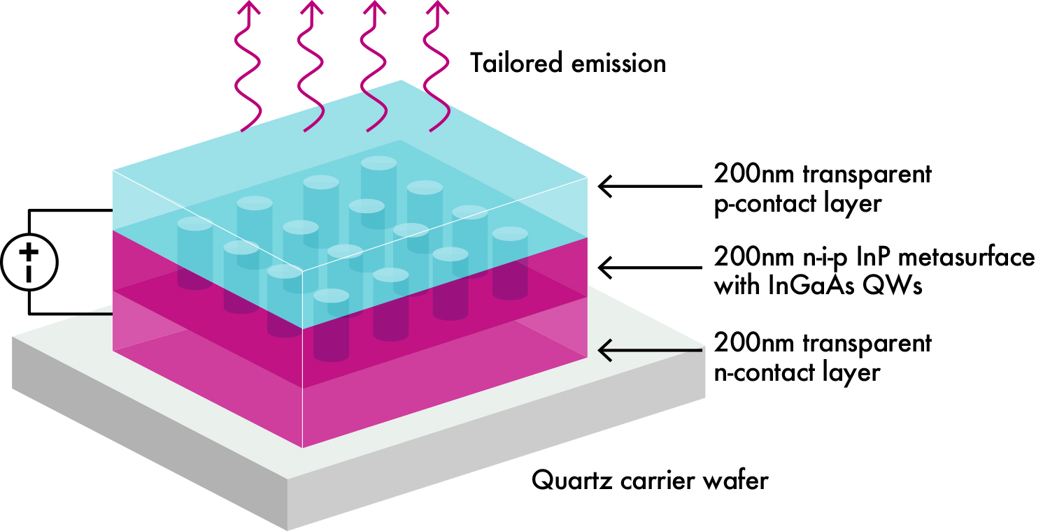
With fabrication processes made possible by ANFF-ACT, Dr Haggren is developing an electrically injected, light-emitting metasurface device. His device is based on an indium phosphide (InP) metasurface film sandwiched between two transparent charge-carrying layers. InP is a semiconductor that emits photons of light when injected with an electrical current. The InP is studded with InGaAs quantum structures that confine charge carriers to tailor the colour of the emitted light. Rather than diffusely glowing like a LED, the light-emitting metasurface produces a coherent nanolaser beam in which the released wavelengths are in exact alignment in space and time.
Engineered metamaterials and coherent beams enable much stronger tunability and reconfigurability than any natural, non-structured material. Haggren’s metasurface nanolaser is a promising candidate for future flat devices that can change various properties of emitted light such as colour, brightness, phase, polarisation and direction.
Arrays of nanoscale emitters can be directed toward the same focal point in space, what would emerge at that location is a 3D object composed solely of light – a true hologram.
Advances in nanoscale emitters will improve various technologies including virtual reality with improved simulated environments for training and education to next generation wireless optical networking technology (called Li-Fi) for ultra-high speed data transmission.