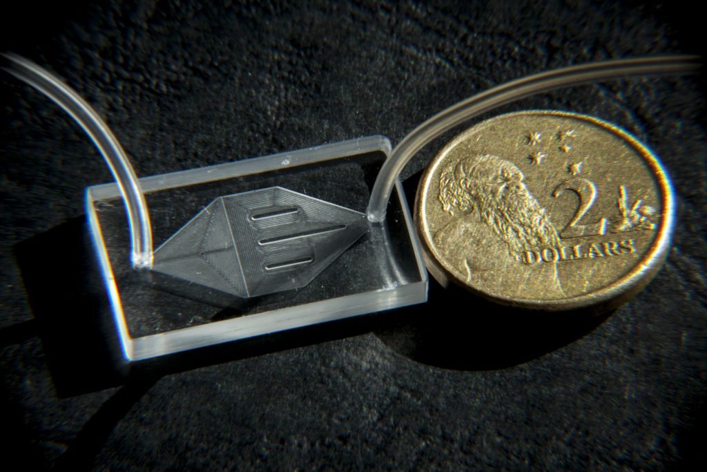
Microfluidic devices
Microfluidic devices use micron-sized channels to precisely manipulate fluids. These channels are typically cut into a substrate of glass, PDMS, or silicon and allow micro, nano, or pico litres of fluids to be exposed to technologies such as sensors, active devices, or lab-on-a-chip environments.
The ease at which microfluidic devices can be taken out of the lab and directly to the point of care mean that the commercial field is rapidly evolving, while also providing an affordable testbed that provides fast results for fundamental research into biomedical treatments.
Researchers are designing new devices for applications ranging from in vitro diagnostics, pharmaceutical research, gene therapy, drug delivery research, organ-on-a-chip technologies, to non-medical applications such as mineral extraction or chemical sensing.
List of Possible Process Flows
Polymer Microfluidic Device with embossing master (medium feature sizes)
Step 1
Step 2
Step 3
Step 4
Step 5
CAD Computers
Professional CAD computing requires serious hardware – certain ANFF sites possess dedicated CAD computers for modelling and designing purposes.
These computers will feature specific software packages to model complex systems such as optical or microfluidic devices, to interpret 3D scanner information, or to…
Computer Numerical Control (CNC) milling
CNC milling is a conventional manufacturing technique that uses a computer to control a milling cutter.
It can be used to precisely machine geometries and features into a substrate, or to mill hot embossing stamps and jigs that may be used to fabricate microstructured features in devices.
The equipment typically…
Hot embossing
Hot embossing is a pattern-transfer technique, involving the application of pressure and heat to a polymeric or resist-coated substrate, placed in contact with a master mould. This allows the relief features on the mould to be transferred faithfully. Hot embossing achieves fast patterning at a resolution of…
Optical microscopy
A fundamental form of sample analysis, optical microscopy uses a series of lenses to focus light that is reflected from or passed through a sample. Various forms of light and magnification can be used to visualise the sample.
Wafer bonding
Bonding a wafer to another wafer is a step commonly used when packaging components in an micro or nanoelectrical device. It can help a form new functions in a device, or can ensure mechanical and hermetic encapsulation of devices and electronics. The result is irreversible.
Common bonding methods include using heat…
Polymer Microfluidic Device
Step 1
Step 2
Step 3
Step 4
CAD Computers
Professional CAD computing requires serious hardware – certain ANFF sites possess dedicated CAD computers for modelling and designing purposes.
These computers will feature specific software packages to model complex systems such as optical or microfluidic devices, to interpret 3D scanner information, or to…
Computer Numerical Control (CNC) milling
CNC milling is a conventional manufacturing technique that uses a computer to control a milling cutter.
It can be used to precisely machine geometries and features into a substrate, or to mill hot embossing stamps and jigs that may be used to fabricate microstructured features in devices.
The equipment typically…
Optical microscopy
A fundamental form of sample analysis, optical microscopy uses a series of lenses to focus light that is reflected from or passed through a sample. Various forms of light and magnification can be used to visualise the sample.
Wafer bonding
Bonding a wafer to another wafer is a step commonly used when packaging components in an micro or nanoelectrical device. It can help a form new functions in a device, or can ensure mechanical and hermetic encapsulation of devices and electronics. The result is irreversible.
Common bonding methods include using heat…
Polymer Microfluidic Device with embossing master (small feature sizes)
Step 1
Step 2
Step 3
Step 4
Step 5
Step 6
CAD Computers
Professional CAD computing requires serious hardware – certain ANFF sites possess dedicated CAD computers for modelling and designing purposes.
These computers will feature specific software packages to model complex systems such as optical or microfluidic devices, to interpret 3D scanner information, or to…
Multiple mask lithography
Photolithography is used to create a pattern on a substrate by shining light from a light source onto a photoresist that coats the surface of the substrate through a photomask and is followed by a development phase.
Depending on the complexity of a device’s design, various deposition, etching and lithography…
PDMS moulding
Polydimethylsiloxane (PDMS) is widely used to create a low-cost micro-structured mould for microfluidic applications.
PDMS is an incredibly well behaved material under a variety of conditions, it’s biocompatible and is very easy to fabricate.
Hot embossing
Hot embossing is a pattern-transfer technique, involving the application of pressure and heat to a polymeric or resist-coated substrate, placed in contact with a master mould. This allows the relief features on the mould to be transferred faithfully. Hot embossing achieves fast patterning at a resolution of…
Confocal microscopy
A confocal microscope records point-by-point scans of a sample to create two-dimensional images.
Three-dimensional images can be created by combining the images of multiple planes, taken by repeating the scanning technique but varying the z-axis.
Wafer bonding
Bonding a wafer to another wafer is a step commonly used when packaging components in an micro or nanoelectrical device. It can help a form new functions in a device, or can ensure mechanical and hermetic encapsulation of devices and electronics. The result is irreversible.
Common bonding methods include using heat…
Glass Microfluidic Device
Step 1
Step 2
Step 3
Step 4
Step 5
CAD Computers
Professional CAD computing requires serious hardware – certain ANFF sites possess dedicated CAD computers for modelling and designing purposes.
These computers will feature specific software packages to model complex systems such as optical or microfluidic devices, to interpret 3D scanner information, or to…
Multiple mask lithography
Photolithography is used to create a pattern on a substrate by shining light from a light source onto a photoresist that coats the surface of the substrate through a photomask and is followed by a development phase.
Depending on the complexity of a device’s design, various deposition, etching and lithography…
Deep Reactive Ion Etching (DRIE)
Deep Reactive Ion Etching (DRIE) is effectively an extension of the Reactive Ion Etching (RIE) process, but can provide higher aspect ratio structures.
The DRIE process alternates between etch and passivation cycles to allow patterns to be cut deeper into a substrate.
Etch channels or other feature geometries with…
Optical microscopy
A fundamental form of sample analysis, optical microscopy uses a series of lenses to focus light that is reflected from or passed through a sample. Various forms of light and magnification can be used to visualise the sample.
Wafer bonding
Bonding a wafer to another wafer is a step commonly used when packaging components in an micro or nanoelectrical device. It can help a form new functions in a device, or can ensure mechanical and hermetic encapsulation of devices and electronics. The result is irreversible.
Common bonding methods include using heat…
Glass Microfluidic Device with electrodes
Step 1
Step 2
Step 3
Step 4
Step 5
Step 6
Step 7
Step 8
CAD Computers
Professional CAD computing requires serious hardware – certain ANFF sites possess dedicated CAD computers for modelling and designing purposes.
These computers will feature specific software packages to model complex systems such as optical or microfluidic devices, to interpret 3D scanner information, or to…
Multiple mask lithography
Photolithography is used to create a pattern on a substrate by shining light from a light source onto a photoresist that coats the surface of the substrate through a photomask and is followed by a development phase.
Depending on the complexity of a device’s design, various deposition, etching and lithography…
Electron Beam Evaporation (E-Beam Evaporation)
Electron-beam evaporation is a physical vapour deposition method for depositing thin films of metals, oxides and semiconductors in a high vacuum environment. Ultra high purity coating material is placed inside a vacuum chamber, typically as pellets in a crucible. Electron energy is used to heat these pellets,…
Reactive Ion Etching (RIE)
Reactive Ion Etching (RIE) is a method that combines both chemical and physical etching to allow isotropic and anisotropic material removal.
The etching process is carried out in a chemically reactive plasma containing positively and negatively charged ions generated from gases that are pumped into the reaction…
Multiple mask lithography
Photolithography is used to create a pattern on a substrate by shining light from a light source onto a photoresist that coats the surface of the substrate through a photomask and is followed by a development phase.
Depending on the complexity of a device’s design, various deposition, etching and lithography…
Deep Reactive Ion Etching (DRIE)
Deep Reactive Ion Etching (DRIE) is effectively an extension of the Reactive Ion Etching (RIE) process, but can provide higher aspect ratio structures.
The DRIE process alternates between etch and passivation cycles to allow patterns to be cut deeper into a substrate.
Etch channels or other feature geometries with…
Optical microscopy
A fundamental form of sample analysis, optical microscopy uses a series of lenses to focus light that is reflected from or passed through a sample. Various forms of light and magnification can be used to visualise the sample.
Wafer bonding
Bonding a wafer to another wafer is a step commonly used when packaging components in an micro or nanoelectrical device. It can help a form new functions in a device, or can ensure mechanical and hermetic encapsulation of devices and electronics. The result is irreversible.
Common bonding methods include using heat…