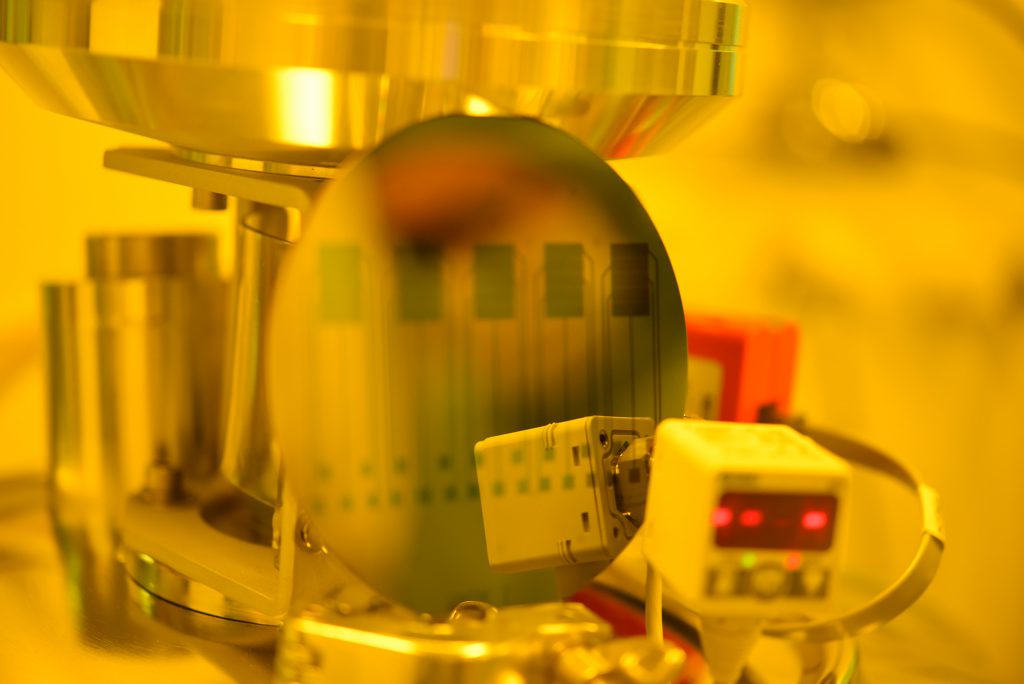
X-ray optics are used to focus, bend, or otherwise manipulate x-rays to meet the needs of certain applications.

Electron Beam Lithography (EBL) allows users to write patterns with extremely high resolution, smaller than 10nm in size. It makes use of a highly energetic, tightly focused electron beam, which is scanned over a sample coated with an electron-sensitive resist. The electron beam scans the image according to a…
Atomic Layer Deposition (ALD) involves the deposition of materials one atomic monolayer at a time. It forms extremely uniform, conformal, pin-hole-free coatings even on high-aspect-ratio structures. This is achieved by pulsing a chemical precursor onto a hydroxylated substrate surface which reacts, resulting in a…
Atomic force microscopy (AFM) is one of the most versatile characterisation methods.
AFM performs scanning probe microscopy, scanning the surface of a material with a nanoscale cantilever, either through direct contact or through oscillating the cantilever just above the surface. When the cantilever is positioned…
Focused Ion Beam (FIB) milling provides significant advantages as a single-step, nanoscale prototyping method that doesn’t require a mask or resist. It is capable of performing: subtractive lithography in which atoms are locally milled away by physical sputtering with sub-10nm resolution; additive lithography in…
Plasma Enhanced Chemical Vapour Deposition (PECVD) uses a plasma to deposit a thin film of silicon dioxide or silicon nitrate onto a substrate. PECVD uses lower temperatures than the furnace systems to achieve an insulating layer on a variety of materials.
PECVD is used in optics, microelectronics, energy…
Deep Reactive Ion Etching (DRIE) is effectively an extension of the Reactive Ion Etching (RIE) process, but can provide higher aspect ratio structures.
The DRIE process alternates between etch and passivation cycles to allow patterns to be cut deeper into a substrate.
Etch channels or other feature geometries with…
Scanning Electron Microscopy (SEM) is the process whereby a tightly focused electron beam is scanned onto the surface to be imaged. As the primary electrons hit the atoms in the surface, a number of secondary electrons are emitted, and collected by the instrument’s detector, which assigns a level of grey…

